Semiconductor device
- Summary
- Abstract
- Description
- Claims
- Application Information
AI Technical Summary
Benefits of technology
Problems solved by technology
Method used
Image

Examples
first embodiment
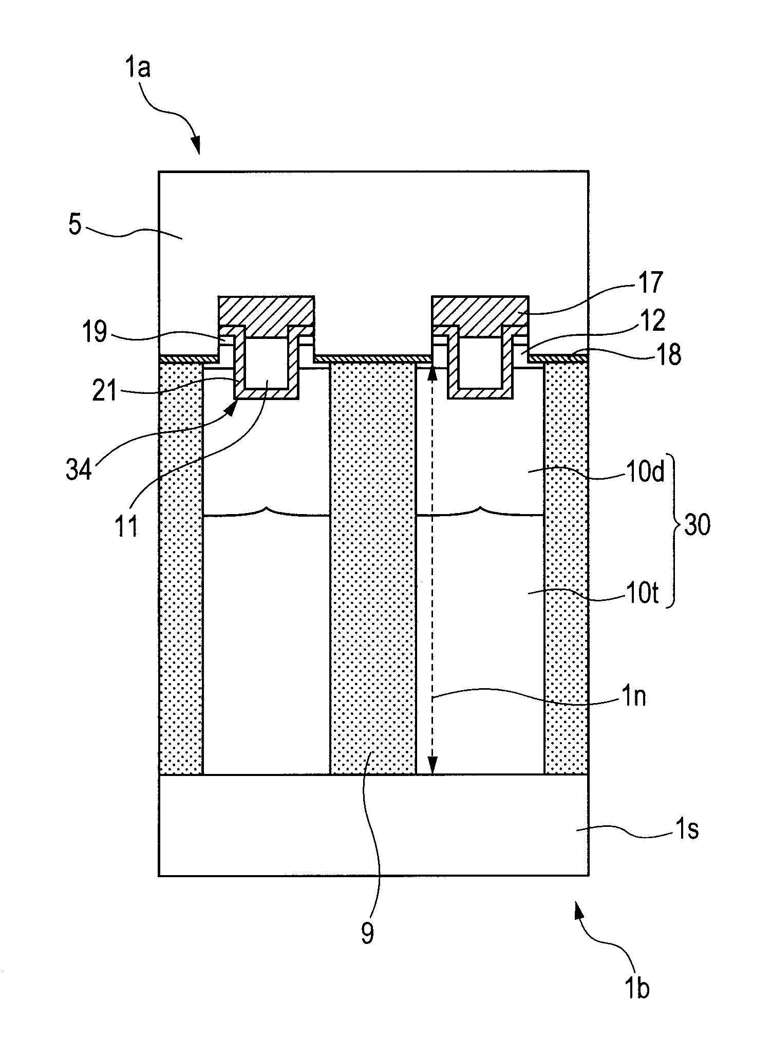
[0131]1. Description of a device structure (N+ / N two-stage conventional epitaxy system) of a planar power MOSFET, which is an example of the semiconductor device according to the present application, (mainly from FIG. 1 to FIG. 6). In this example, a planar power MOSFET fabricated over a silicon semiconductor substrate and having a source-drain breakdown voltage of about 600 V will be described specifically (a planar power MOSFET is similar to it in the following sections). It is however needless to say that the description can be applied to a power MOSFET or another device having a breakdown voltage different from the above one.
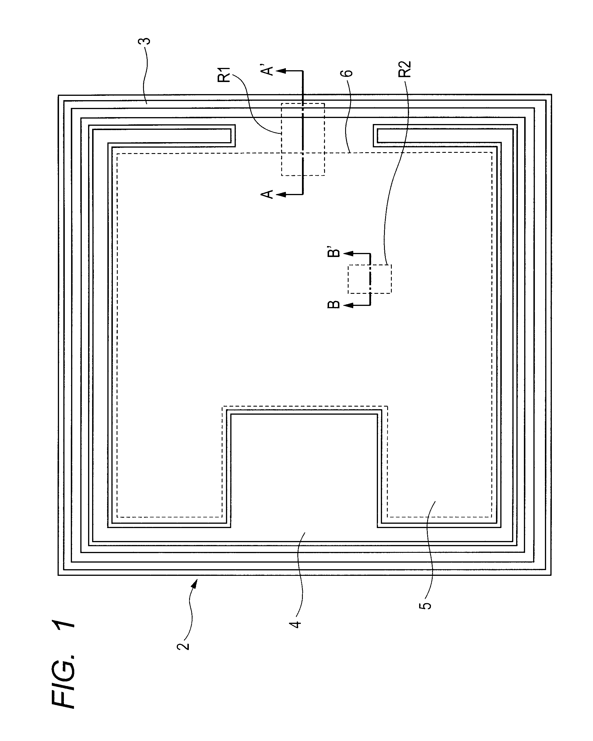
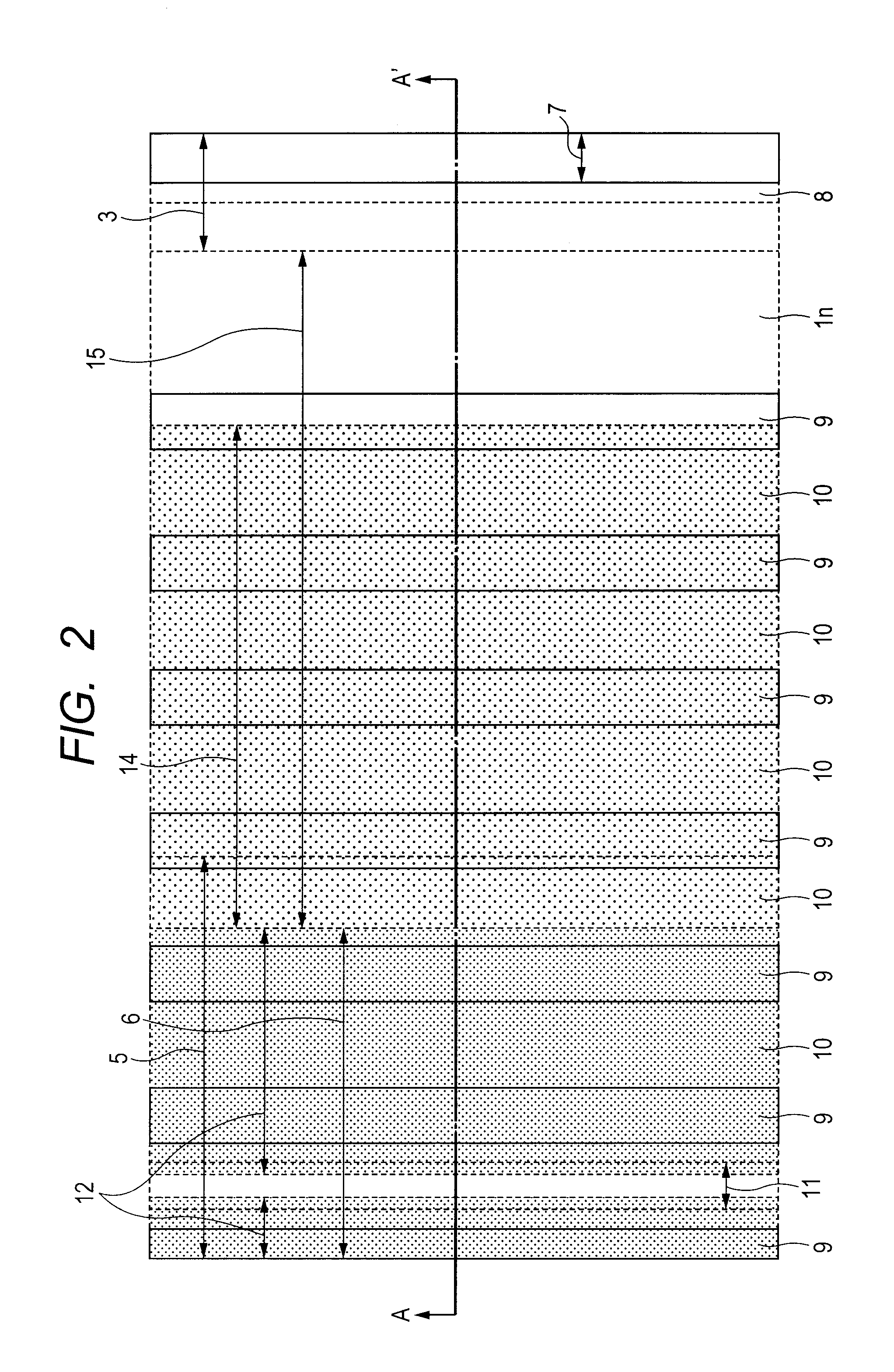
[0132]FIG. 1 is an overall top view of a semiconductor chip (silicon-based member chip) according to a first embodiment (common to each embodiment) of the present application. FIG. 2 is an enlarged plan view of an internal structure corresponding to a cutout portion R1 of the regions of an active cell end portion and a chip peripheral portion illustrated in ...
second embodiment
[0159]3. Description of a device structure (N / N-two-stage conventional epitaxy system) of a planar power MOSFET, which is an example of a semiconductor device according to the present application (mainly FIGS. 35 and 36) The following example is a modification example (having the N type upper-layer silicon epitaxial layer 1d thicker than the N type lower-layer silicon epitaxial layer 1t) of the N type silicon epitaxial structure in the active cell structure (FIG. 5) and in the whole region (the N type lower-layer silicon epitaxial layer 1t and the N type upper-layer silicon epitaxial layer 1d illustrated in FIG. 3) described in Sections 1 and 2 (having the N type upper-layer silicon epitaxial layer 1d thinner than the N type lower-layer silicon epitaxial layer 1t). In the active cell region, the modification appears in the drift region 30, while in a region other than the active cell region, modification appears only in the N type silicon epitaxial layer 1n so that only the active c...
fourth embodiment
[0169]6. Description of the major part of a wafer process in the manufacturing method of a semiconductor device according to the present application (referring mainly to FIGS. 41 to 44). In this section, the major part of the process corresponding to the active cell region described in Section 5 will be described. The fundamental portions are similar to those described in Section 2 so that only a different portion will next be described.
[0170]FIG. 41 is a device cross-sectional view (a step of patterning a hard mask film for opening a P-column trench) illustrating a process flow (the fourth embodiment) corresponding to the device cross-section illustrated in FIG. 39. FIG. 42 is a device cross-sectional view (a step of obliquely implanting ions into an N-column region) illustrating the process flow (the fourth embodiment) corresponding to the device cross-section illustrated in FIG. 39. FIG. 43 is a device cross-sectional view (an epitaxy trench filling step) illustrating the process...
PUM
 Abstract
Description
Claims
Application Information
 - R&D Engineer
- R&D Manager
- IP Professional
- Industry Leading Data Capabilities
- Powerful AI technology
- Patent DNA Extraction
Browse by: Latest US Patents, China's latest patents, Technical Efficacy Thesaurus, Application Domain, Technology Topic.
© 2024 PatSnap. All rights reserved.Legal|Privacy policy|Modern Slavery Act Transparency Statement|Sitemap