Power connection structure of driver IC chip

a technology of driver ic chip and power connection structure, which is applied in the direction of electric digital data processing, instruments, computing, etc., can solve the problems of affecting the economic benefits of the system, affecting the efficiency of the system, so as to reduce the size of the driver ic chip and the manufacturing cost of the system. , the effect of simplifying the wiring lin

Active Publication Date: 2011-10-13
SILICON WORKS CO LTD
View PDF3 Cites 7 Cited by
  • Summary
  • Abstract
  • Description
  • Claims
  • Application Information

AI Technical Summary

Benefits of technology

Accordingly, the present invention has been made in an effort to solve the problems occurring in the related art, and an object of the present invention is to provide a power connection structure of a driver IC chip, in which routing patterns in a driver IC chip are disposed parallel to LOGs (lines-on-glass) to connect power terminal units disposed on both ends of the driver IC chip, thereby simplifying wiring lines and reducing line resistance.
In the power connection structure of a driver IC chip according to the present invention, since the number of wiring lines of input / output terminals of a driver IC chip is decreased, wiring lines can be simplified, and due to this fact, the size of the driver IC chip and the manufacturing cost thereof can be reduced.
Also, in the present invention, advantages are provided in that, since routing patterns in the driver IC chip are disposed in parallel to LOGs to connect power terminal units with each other, line resistance can be reduced and signal delay can be diminished.

Problems solved by technology

If a power source is disposed only in one side of the driver IC chip, since signals may become weak on the other side with no power source, operational problems may be caused.
However, because the power sources disposed on both sides of the driver IC chip should be connected with each other by separate connection lines on flexible printed circuits (FPCs), input / output wiring lines become complicated on the FPCs.
Also, since the wiring lines are added, economy may deteriorate.
Moreover, in the conventional COG mounting type, a disadvantage is caused in that a voltage drop is likely to occur due to inherent resistance of a signal or power supply line composed of a metal line.

Method used


Image

  • Power connection structure of driver IC chip
  • Power connection structure of driver IC chip
  • Power connection structure of driver IC chip

Examples


Embodiment Construction

Reference will now be made in greater detail to a preferred embodiment of the invention, an example of which is illustrated in the accompanying drawings. Wherever possible, the same reference numerals will be used throughout the drawings and the description to refer to the same or like parts.

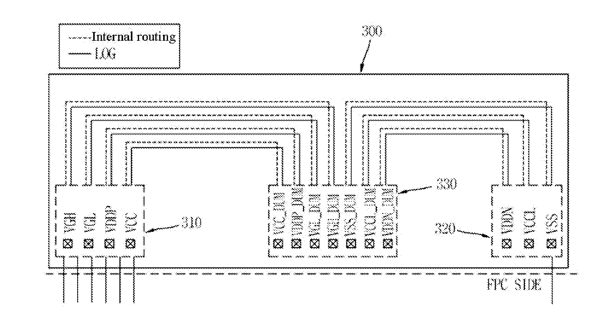
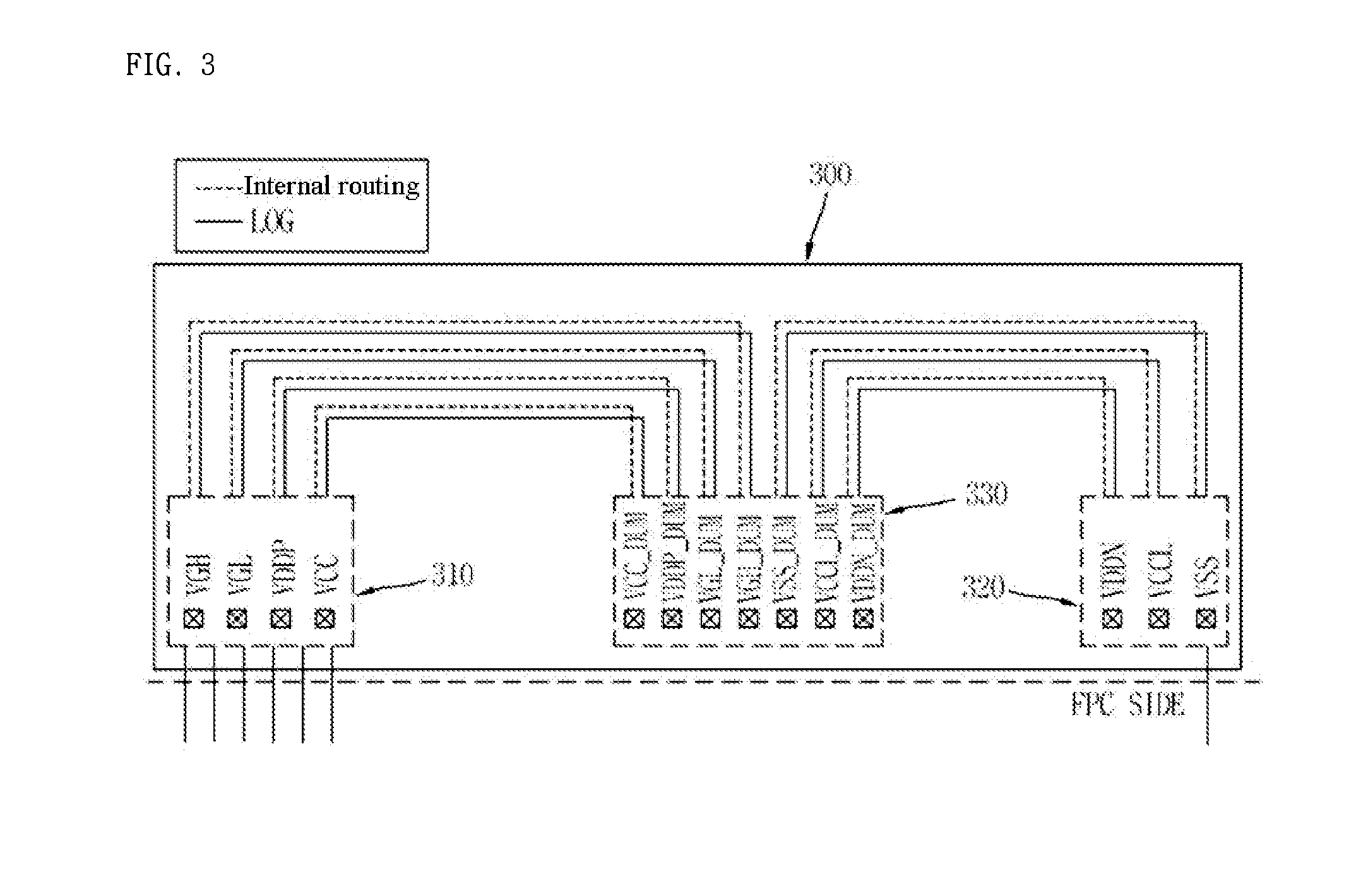
FIG. 3 is a diagram illustrating a power connection structure of a driver IC chip in accordance with an embodiment of the present invention.

Referring to FIG. 3, in the embodiment of the present invention, a driver IC chip 300 includes a first power terminal unit 310 formed on one side thereof, a second power terminal unit 320 formed on the other side thereof, and a dummy power terminal unit 330 formed between the first power terminal unit 310 and the second power terminal unit 320.

The first power terminal unit 310 and the second power terminal unit 320 include power terminals VGH and VGL for supplying gate driving voltages or power terminals VDDP, VCC, VCCL and VSS for supplying source driving v...


PUM


Abstract

A power connection structure of a driver IC chip including a first power terminal unit formed on one side thereof, a second power terminal unit formed on the other side thereof, and a dummy power terminal unit formed between the first power terminal unit and the second power terminal unit. The driver IC chip is mounted to a liquid crystal panel of a liquid crystal display device in a chip-on-glass (COG) type. Both of the first power terminal unit and the dummy power terminal unit and both of the dummy power terminal unit and the second power terminal unit are connected through routing lines in the driver IC chip.

Description

BACKGROUND OF THE INVENTION1. Field of the InventionThe present invention relates to a power connection structure of a driver IC (integrated circuit) chip, and more particularly, to a power connection structure of a driver IC chip, in which routing patterns in a driver IC chip are disposed parallel to LOG (line-on-glass) type lines to connect power terminal units disposed on both ends of the driver IC chip, thereby simplifying wiring lines and reducing line resistance.2. Description of the Related ArtA liquid crystal display (LCD) means a device which uses a characteristic that an aligned state of liquid crystal molecules is changed depending upon an applied voltage and image data is displayed by passing light through liquid crystals. Recently, a most actively used device among liquid crystal displays is a thin film transistor type liquid crystal display (TFT-LCD) which is made by using a silicon IC manufacturing technology.FIG. 1 is a diagram schematically illustrating the structur...

Claims


Application Information

Patent Timeline
Patent Type & Authority Applications(United States)
IPC IPC(8): G06F3/038
CPCG09G3/3648G09G2300/0413G09G2330/02G09G2320/0223G09G2300/0426G02F1/133G02F1/1345G09G3/36
Inventor AHN, YONG-SUNGLEE, JONG-SOOSHIN, YU-NAKIM, YONG-SUK
Owner SILICON WORKS CO LTD
Why Eureka
Try Eureka