

Anisotropic conductive film and light emitting device
a technology of anisotropic conductive film and light-emitting device, which is applied in the direction of film/foil adhesives without carriers, film/foil adhesives, transportation and packaging, etc. it can solve the problems of deteriorating emission efficiency of led elements b>33/b>, 400 to 500 nm wavelength, and absorbing gold wire on the upper face side, etc., to achieve the effect of not deteriorating the emission efficiency of the light-e-
- Summary
- Abstract
- Description
- Claims
- Application Information
AI Technical Summary
Benefits of technology
Problems solved by technology
Method used
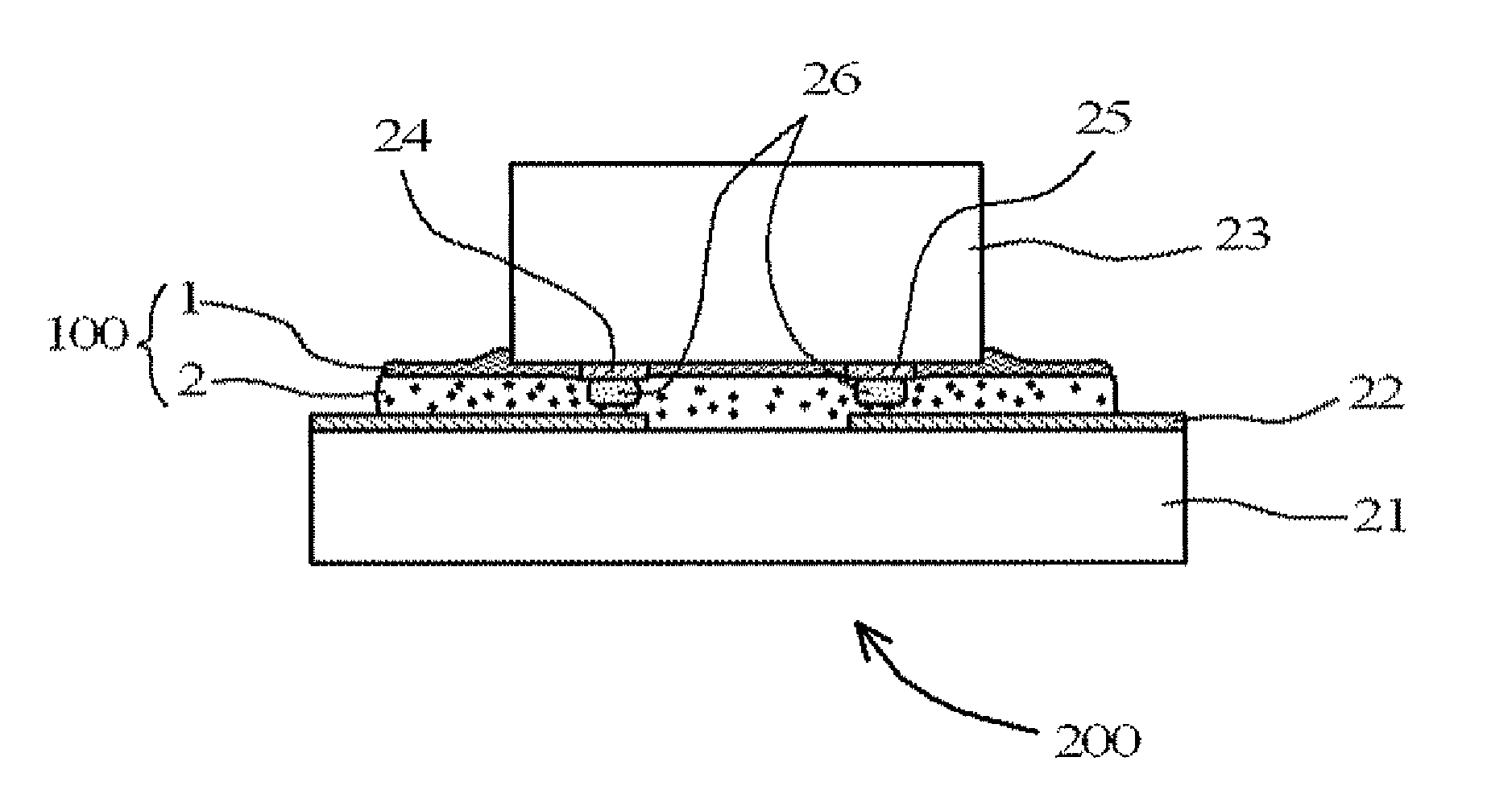
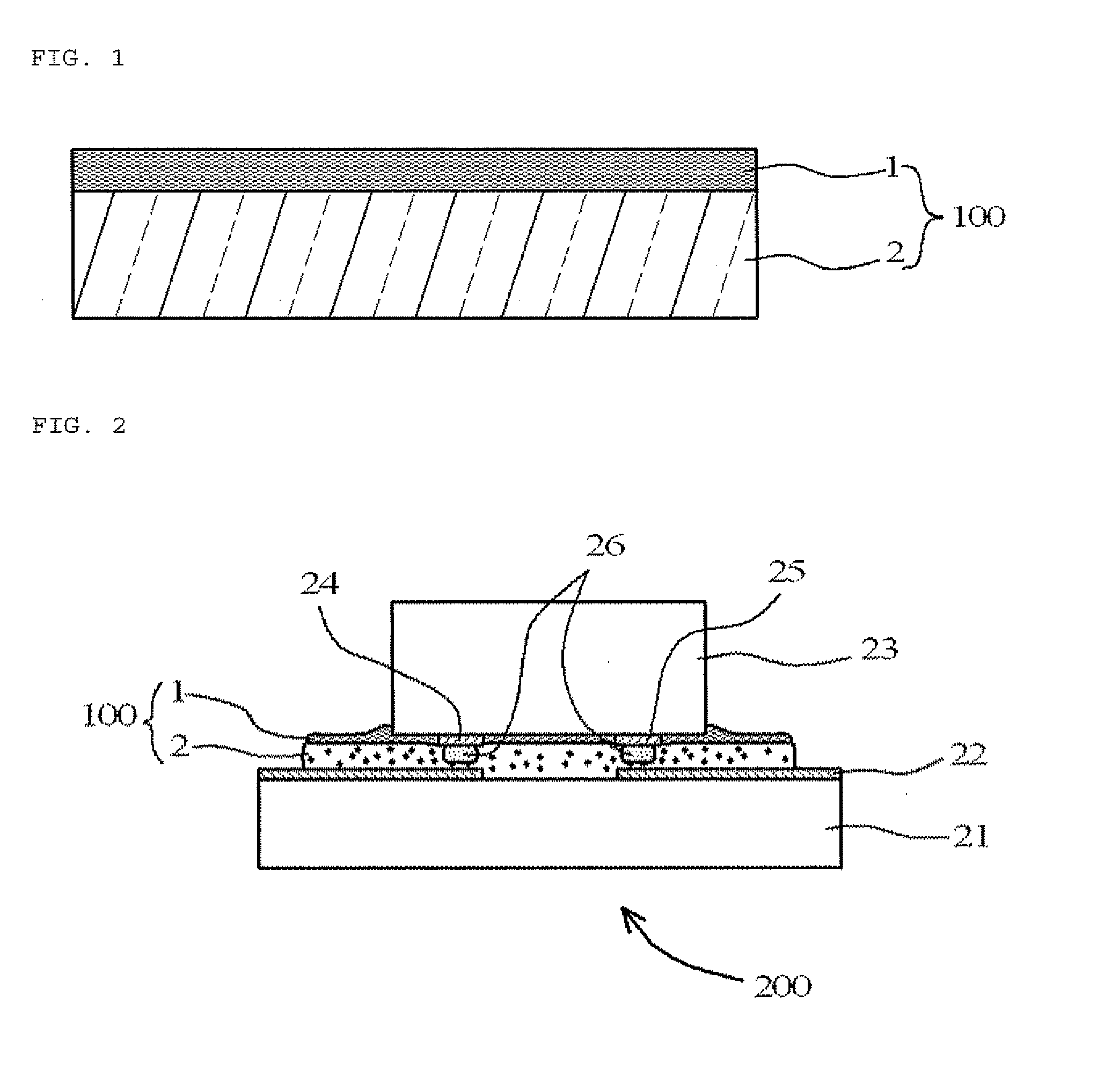
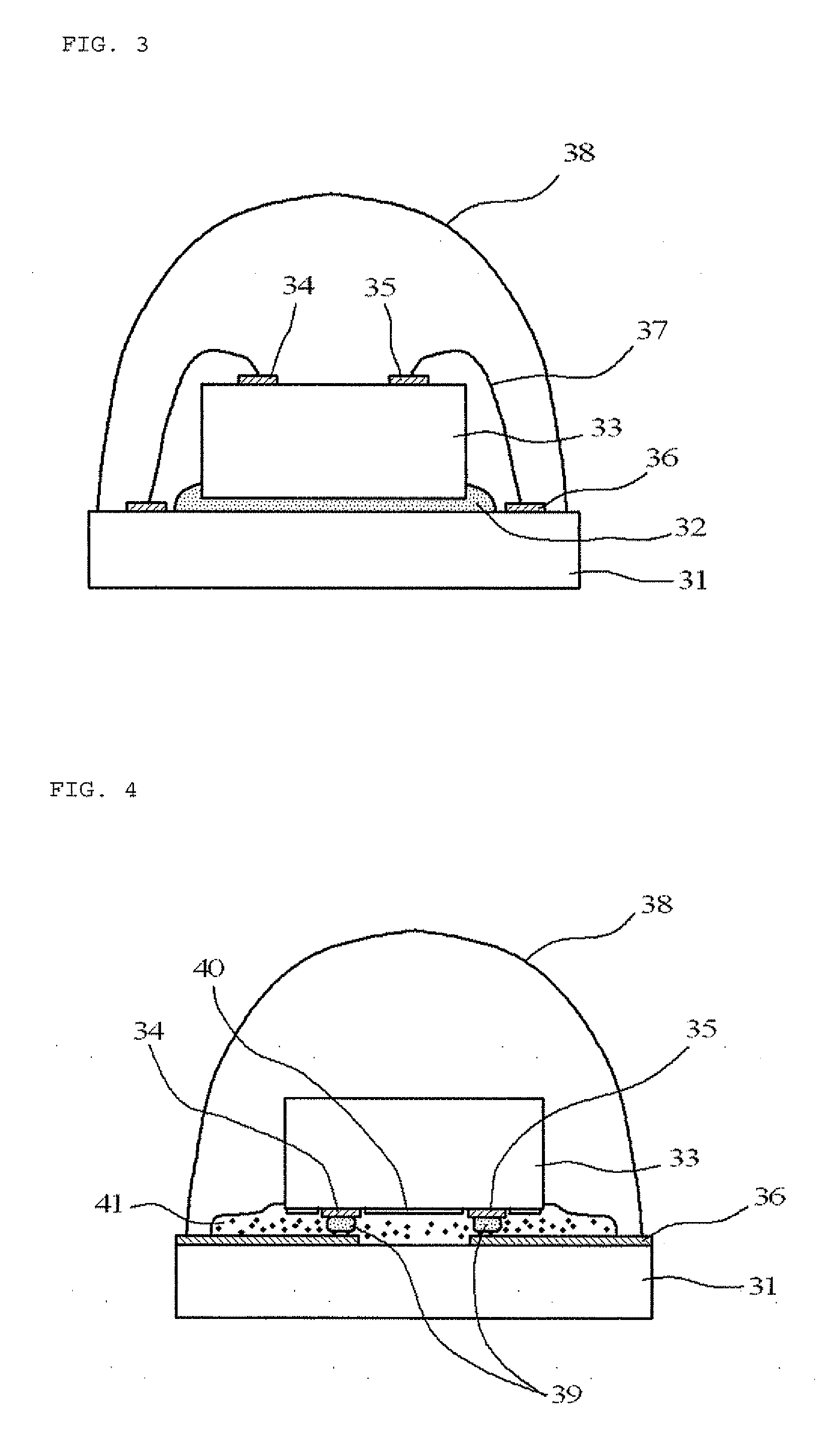
Image

Examples
example 1
(1a) Production of Light-Reflecting Particles
[0031]A flask equipped with a stirring device was charged with 5 g of scale-like silver particles (height 10 μm, width 10 μm, thickness 0.5 μm) and 50 ml of toluene. Then, while stirring, 0.25 g of a silane coupling agent (3-methacryloxypropyltriethoxysilane) was added to the mixture, and the resultant mixture was stirred at 25° C. for 60 minutes. Next, 2 g of methyl methacrylate, 2 g of 2-hydroxyethyl methacrylate, 0.04 g of benzoyl peroxide, and 1 g of 2,4-tolylene diisocyanate was added to the mixture. The resultant mixture was stirred at 80° C. for 12 hours to obtain scale-like silver particles having an insulating coating as light-reflecting particles. The average size of the light-reflecting particles including the insulating coating was a height of 10 μm, a width of 10 μm, and a thickness of 0.5 μm.
(1b) Production of Light-Reflecting Insulating Adhesive Layer Film
[0032]An acid anhydride (MH-700, New Japan Chemical Co., Ltd.) and an...
example 2
[0037]A light-reflecting insulating adhesive layer film and an anisotropic conductive adhesive layer film were produced in the same manner as in Example 1, except that 50 parts by mass of titanium dioxide particles (JR405, Tayca Corporation) having an average particle size of 0.2 μm were used as the light-reflecting particles instead of the scale-like silver particles having an insulating coating. In addition, an anisotropic conductive film was also produced in the same manner as in Example 1. Using this anisotropic conductive film, a light emitting diode element was connected to a glass epoxy substrate, and the properties were evaluated, in the same manner as in Example 1. The obtained results are shown in Table 1.
PUM
| Property | Measurement | Unit |
|---|---|---|
| wavelength | aaaaa | aaaaa |
| particle size | aaaaa | aaaaa |
| particle size | aaaaa | aaaaa |
Abstract
Description
Claims
Application Information