TFET with Nanowire Source
a technology of transistors and nanowires, applied in transistors, nanoinformatics, solid-state devices, etc., can solve the problems of relatively inefficient devices and tfet o
- Summary
- Abstract
- Description
- Claims
- Application Information
AI Technical Summary
Benefits of technology
Problems solved by technology
Method used
Image
Examples
Embodiment Construction
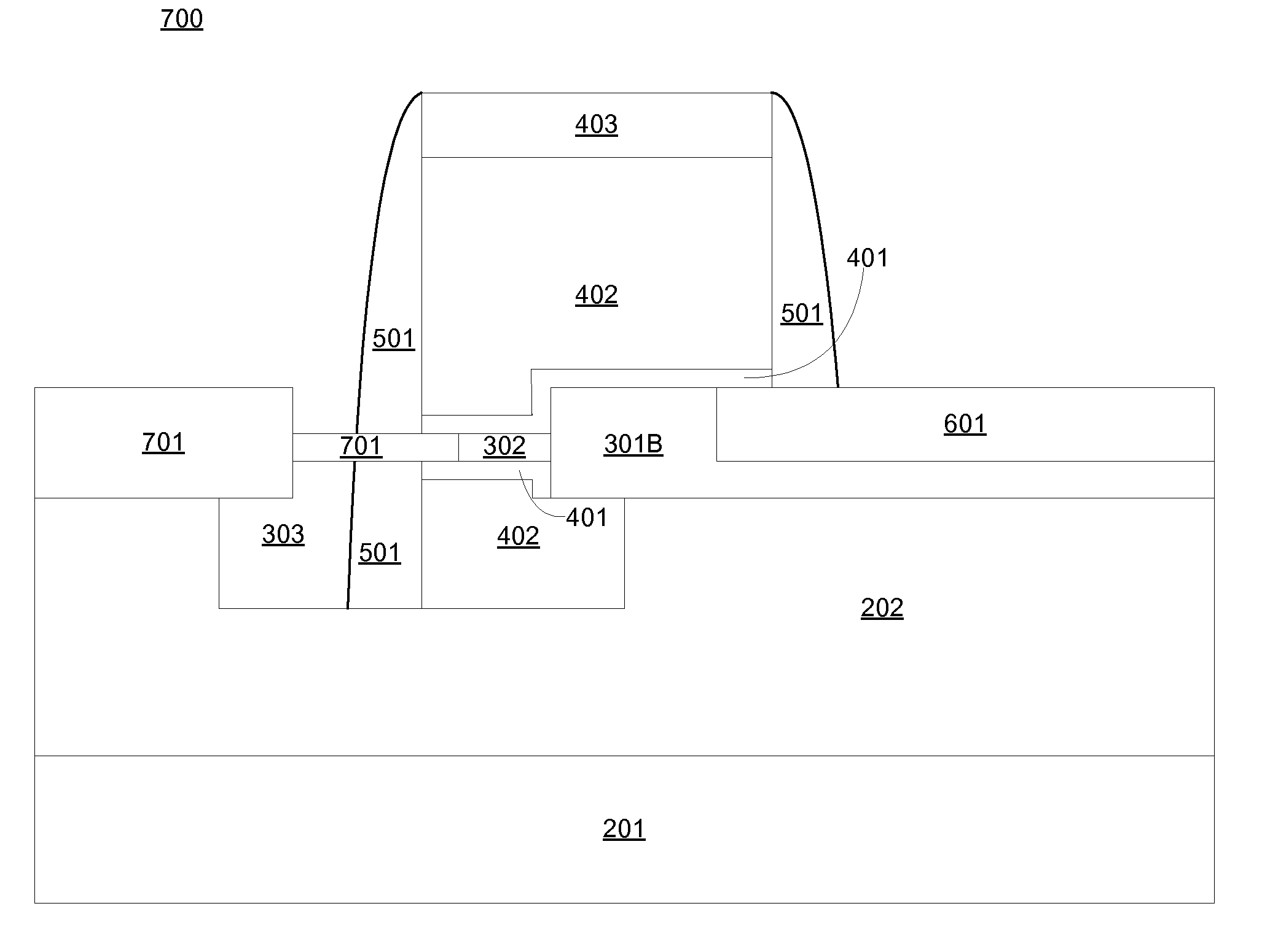
[0015]Embodiments of systems and methods for a TFET with a nanowire source are provided, with exemplary embodiments being discussed below in detail. The TFET source injection point may be located in a GAA nanowire, and the drain may be located in a planar single-gated region. This configuration suppresses ambipolar behavior in the TFET, thereby reducing the TFET off current.
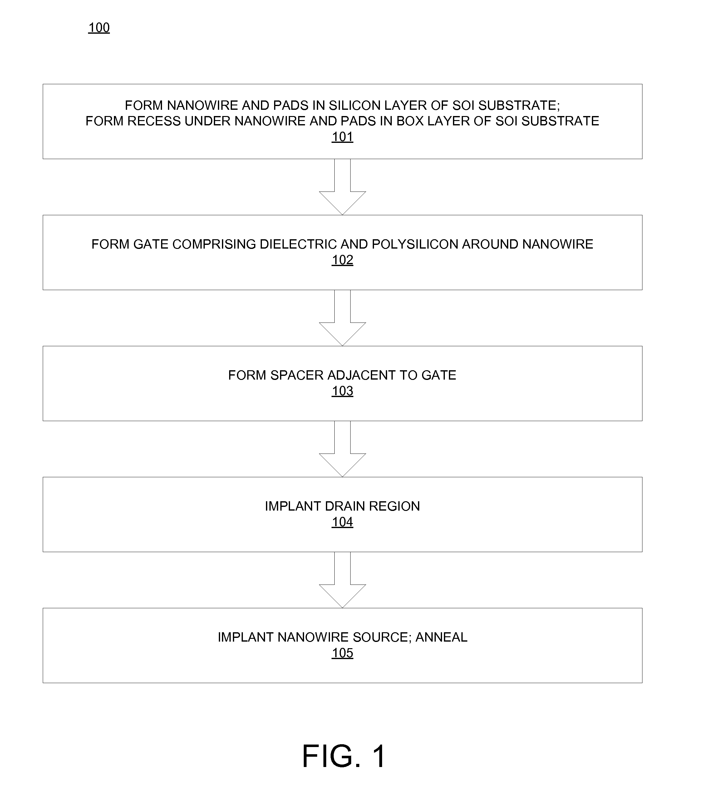
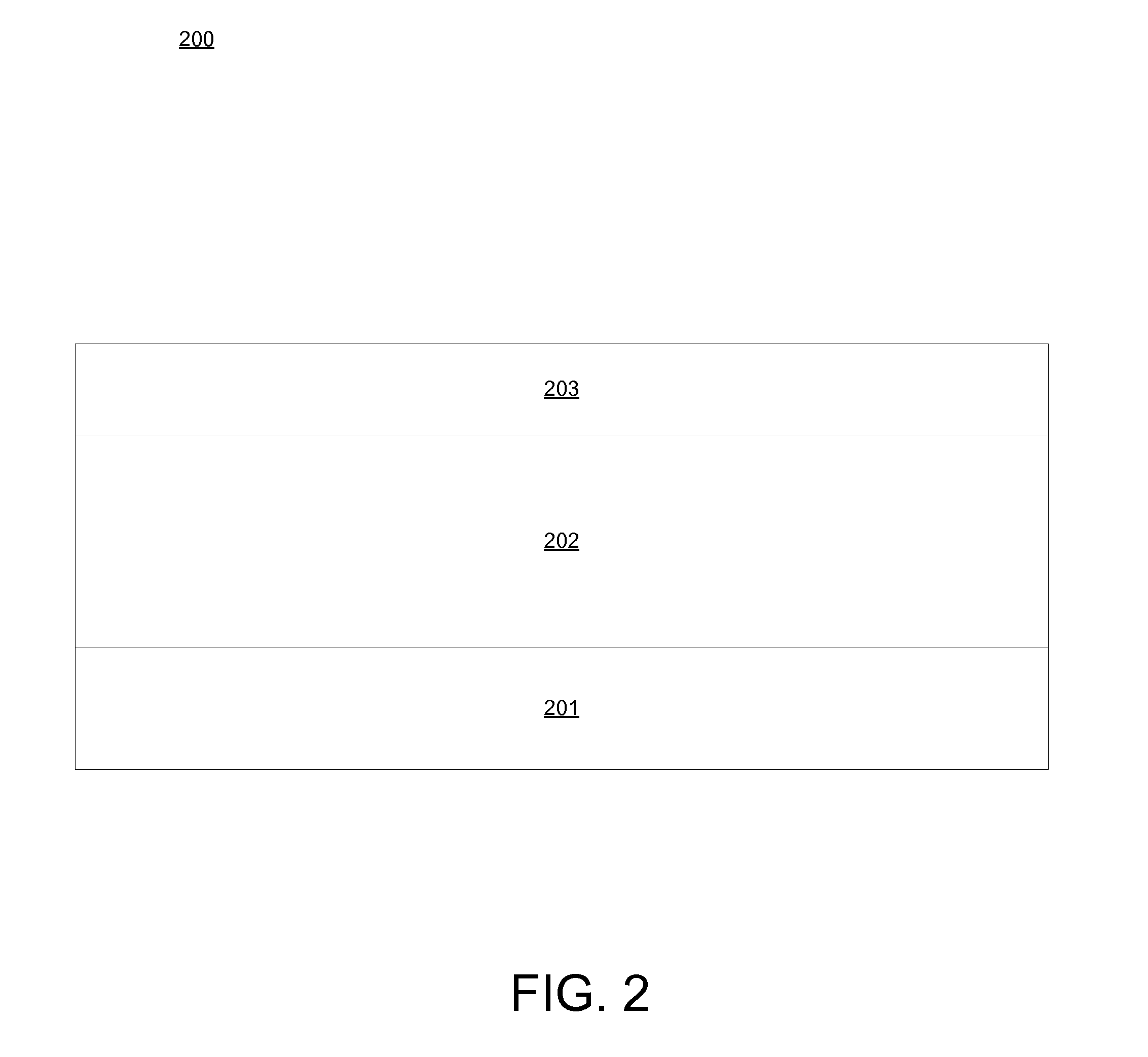
[0016]FIG. 1 illustrates an embodiment of a method of forming a TFET with a nanowire source. FIG. 1 is discussed with reference to FIGS. 2-7. In block 101, a SOI wafer 200 as shown in FIG. 2 is used to form a structure 300 comprising a silicon nanowire 302 as shown in FIG. 3. SOI wafer 200 comprises silicon substrate 201 under buried oxide (BOX) 202 under silicon layer 203. To form nanowire 302, the locations of nanowire 302 and silicon pads 301A-B are lithographically defined and etched in silicon layer 203. After nanowire 302 and silicon pads 301A-B are etched, a portion of BOX 202 is removed to form recess 303...
PUM
 Abstract
Description
Claims
Application Information


