Thin-film transistor, array substrate having the same and method of manufacturing the same

a thin film transistor and array substrate technology, applied in transistors, electrical devices, semiconductor devices, etc., can solve the problems of a-si tft having relatively low charge mobility, a-si tft's manufacturing cost is higher than that of a-si tft, and the threshold voltage can vary with time, so as to reduce the threshold voltage in accordance with time.

Active Publication Date: 2011-11-24
SAMSUNG DISPLAY CO LTD
View PDF5 Cites 39 Cited by
  • Summary
  • Abstract
  • Description
  • Claims
  • Application Information

AI Technical Summary

Benefits of technology

[0027]Embodiments of the invention concern themselves with fabricating and / or using a TFT that has a double gate structure in which gate electrodes are formed both above and below a semiconductor pattern, so that a variation of a threshold voltage in accordance with a time is decreased.

Problems solved by technology

However, the a-Si TFT has relatively low charge mobility.
However, the poly-Si TFT liquid crystal display (LCD) has a more complex manufacturing process than the a-Si TFT, so that its manufacturing cost is higher than that of the a-Si TFT.
However, the oxide semiconductor TFT requires a bias voltage to be applied to one electrode, resulting in threshold voltage that can vary with time.
This reduces the electrical stability and reliability of the switching element.

Method used


Image

  • Thin-film transistor, array substrate having the same and method of manufacturing the same
  • Thin-film transistor, array substrate having the same and method of manufacturing the same
  • Thin-film transistor, array substrate having the same and method of manufacturing the same

Examples


Embodiment Construction

[0039]Hereinafter, the present invention will be explained in detail with reference to the accompanying drawings.

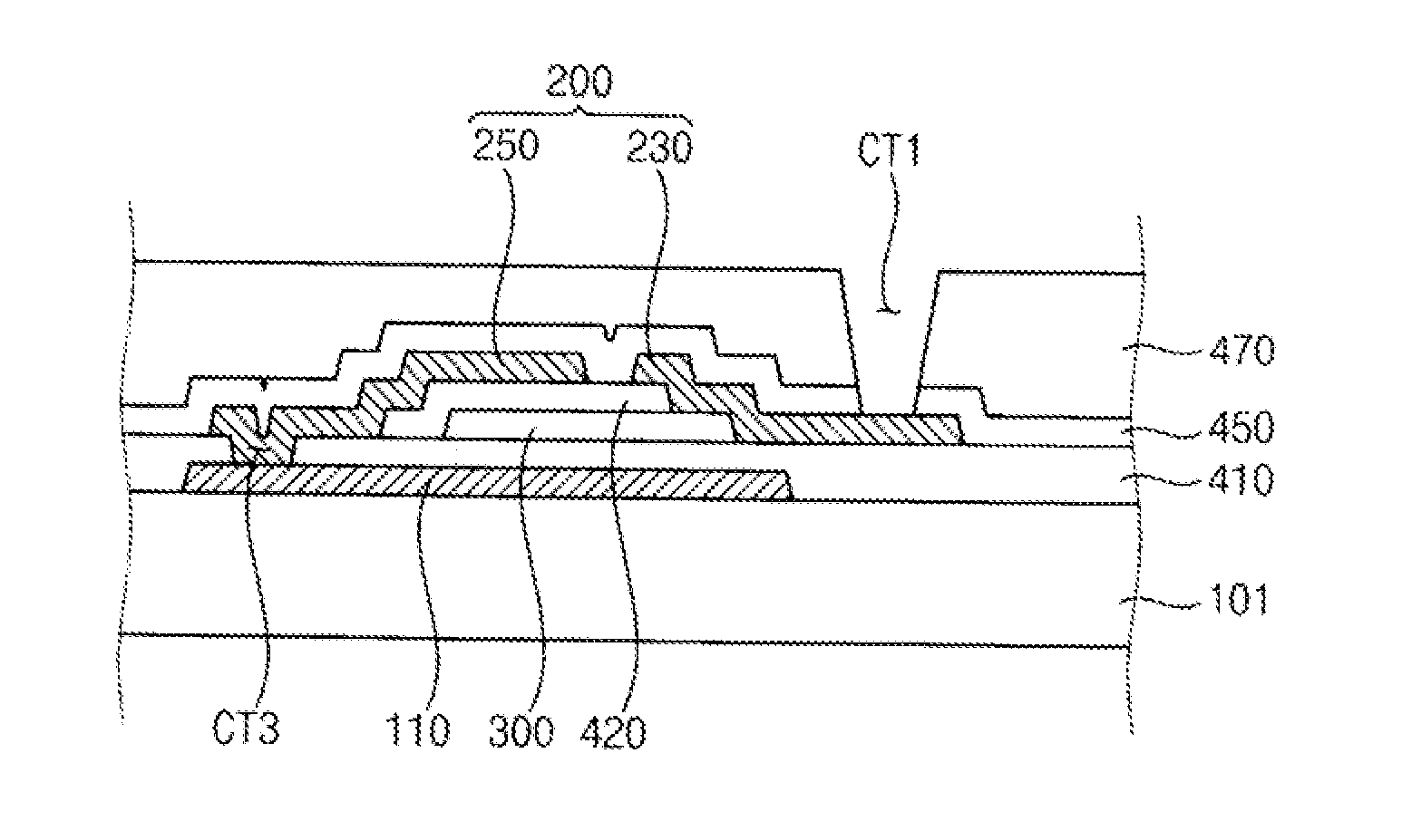
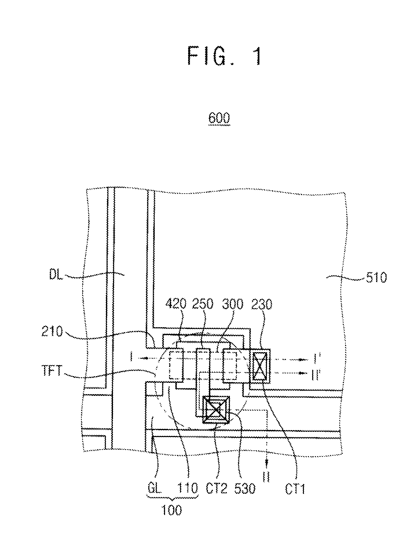
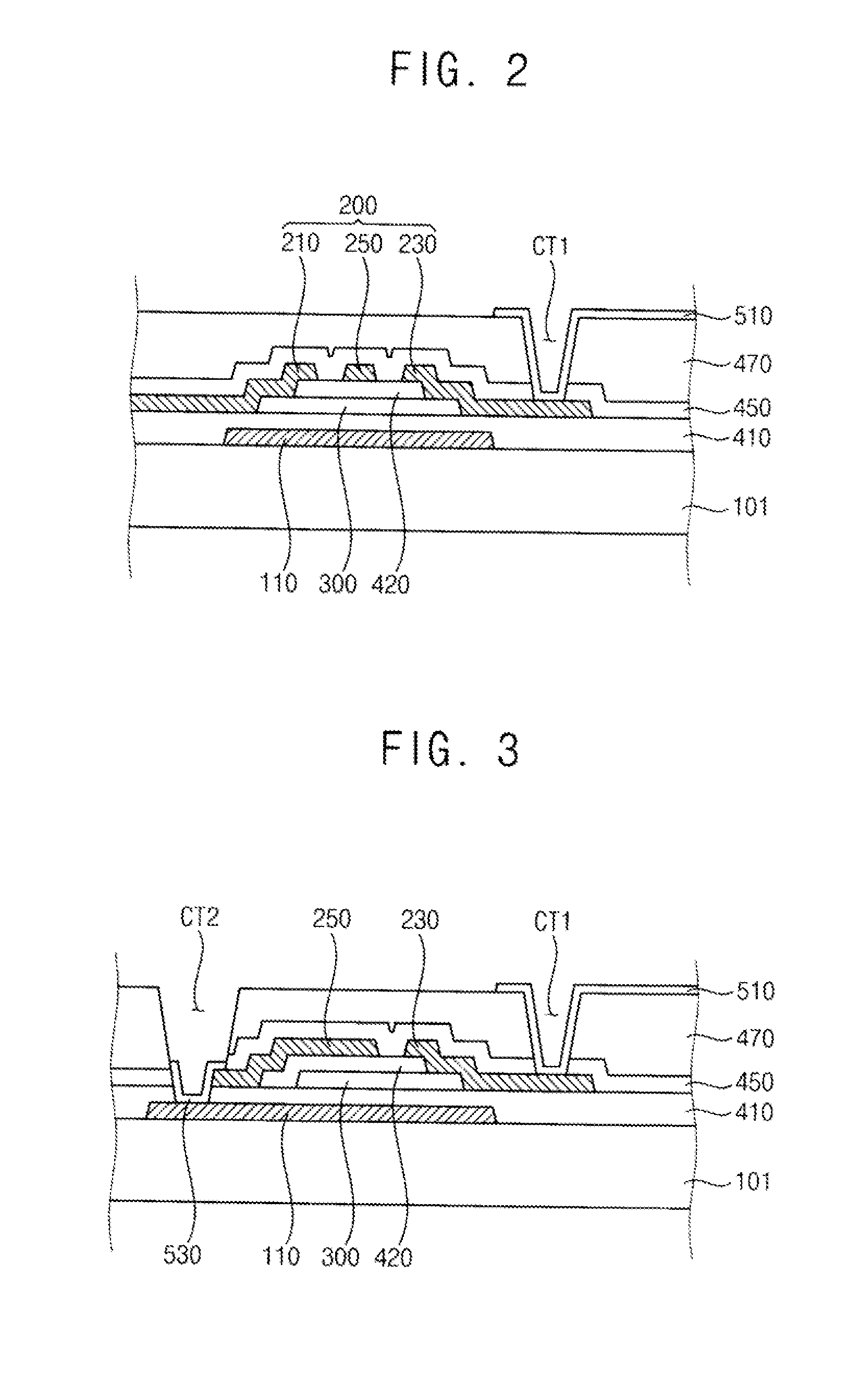
[0040]FIG. 1 is a plan view illustrating an array substrate according to an exemplary embodiment of the present invention. FIG. 2 is a cross-sectional view taken along a line I-I′ of FIG. 1. FIG. 3 is a cross-sectional view taken along a line II-II′ of FIG. 1.

[0041]Referring to FIGS. 1, 2 and 3, the array substrate includes a gate line GL, a data line DL, a thin-film transistor (“TFT”) and a pixel electrode 510.

[0042]The TFT includes a first gate electrode 110, a first gate insulation layer 410, a semiconductor pattern 300, a second gate insulation layer 420, a source electrode 210, a drain electrode 230 and a second gate electrode 250.

[0043]The first gate electrode 110 is electrically connected to the gate line GL. More specifically, the first gate electrode 110 may be an extension protruding from the gate line GL. In this case, the first gate electrode 110 is formed to ...


PUM


Abstract

A thin-film transistor includes a semiconductor pattern, a first gate electrode, a source electrode, a drain electrode and a second gate electrode. The semiconductor pattern is formed on a substrate. A first conductive layer has a pattern that includes the first gate electrode which is electrically insulated from the semiconductor pattern. A second conductive layer has a pattern that includes a source electrode electrically connected to the semiconductor pattern, a drain electrode spaced apart from the source electrode, and a second gate electrode electrically connected to the first gate electrode. The second gate electrode is electrically insulated from the semiconductor pattern, the source electrode and the drain electrode.

Description

PRIORITY STATEMENT[0001]This application claims priority under 35 U.S.C. §119 to Korean Patent Application No. 2010-47341, filed on May 20, 2010 in the Korean Intellectual Property Office (KIPO), the contents of which are herein incorporated by reference in their entirety.BACKGROUND OF THE INVENTION[0002]1. Field of the Invention[0003]Example embodiments of the present invention relate generally to thin-film transistor (“TFT”) arrays. More particularly, example embodiments of the present invention relate to a TFT with decreased variation in threshold voltage and improved electrical reliability, an array substrate having the TFT, and a method of manufacturing the TFT.[0004]2. Description of the Related Art[0005]Generally, flat panel display devices include an array substrate with a number of switching elements and a counter substrate opposite to the array substrate. Each switching element includes a gate electrode connected to a gate line, a semiconductor pattern electrically insulat...

Claims


Application Information

Patent Timeline
Patent Type & Authority Applications(United States)
IPC IPC(8): H01L29/786H01L21/336
CPCH01L27/1225H01L29/78645H01L27/124H01L29/7869H01L29/78648H01L27/1214H01L27/1288
Inventor KIM, KI-WONYOON, KAP-SOOLEE, WOO-GEUNKWON, YEONG-KEUNRYU, HYE-YOUNGLEE, JIN-WONLEE, HYUN-JUNG
Owner SAMSUNG DISPLAY CO LTD
Why Eureka
Try Eureka