Oxide semiconductor devices, methods of manufacturing oxide semiconductor devices, display devices having oxide semiconductor devices, methods of manufacturing display devices having oxide semiconductor devices

a technology of oxide semiconductor and display device, which is applied in the direction of semiconductor devices, electrical devices, transistors, etc., can solve the problems of gate insulation layer etching damage easily generated on the surface of the gate insulation layer, gate insulation layer is frequently contaminated, and the voltage-current characteristics of the transistor may be deteriorated, etc., to achieve improved operation current, increase charge mobility, and enhance electrical characteristics

Inactive Publication Date: 2012-11-22
SAMSUNG DISPLAY CO LTD
View PDF5 Cites 37 Cited by
  • Summary
  • Abstract
  • Description
  • Claims
  • Application Information

AI Technical Summary

Benefits of technology

[0040]According to example embodiments of the present invention, the recess structure may be provided on the gate insulation layer between the source and drain electrodes by performing at least one of the plasma treatment and the cleaning treatment, so that an internal stress generated in forming the source and drain electrodes may be removed from the gate insulation layer. Additionally, a portion of the gate insulation layer damaged by the etching process and etching by-products including metal compounds and / or metallic particles may be effectively removed from the gate insulation layer. Therefore, a channel region of the oxide semiconductor device may be uniformly formed in the active pattern filling the recess structure on the gate insulation layer, such that the oxide semiconductor device may have enhanced electrical characteristics such as an improved operation current, an increased charge mobility, an decreased threshold voltage variation, etc. Furthermore, the charge mobility and the operation current of the oxide semiconductor device may be further enhanced because the gate insulation layer may have a small thickness reduced by the recess structure. When the oxide semiconductor device is employed in a display device such as an organic light emitting display device, a liquid crystal display device or a flexible display device, the display device may have various advantages, for example, a reduced thickness, an increased operation speed, an enhanced quality of displayed images, etc.

Problems solved by technology

When an active layer is formed on a gate insulation layer having internal stress, voltage-current characteristics of the transistor may be deteriorated.
Additionally, etching damage is easily generated on a surface of the gate insulation layer while patterning the metal layer for forming the source and drain electrodes.
Furthermore, the gate insulation layer is frequently contaminated by etching such as metal compounds and metallic particles generated in an etching process for the metal layer.
Thus, an interface between the active layer and the gate insulation layer may be irregular, thereby deteriorating electrical characteristics of the transistor.
For example, the transistor may have poor electrical characteristics such as increased variation of threshold voltages (Vth), decreased charge mobility, reduced operation current (Ion), etc.
When an oxide semiconductor device includes a gate insulation layer having an internal stress, etching damage, and / or etching by-products remaining thereon, the oxide semiconductor device may have deteriorated electrical characteristics, such that the oxide semiconductor devices having the deteriorated electrical characteristics may not be suitable for use in display devices such as a liquid crystal display (LCD) device or an organic light emitting display (OLED) device.

Method used


Image

  • Oxide semiconductor devices, methods of manufacturing oxide semiconductor devices, display devices having oxide semiconductor devices, methods of manufacturing display devices having oxide semiconductor devices
  • Oxide semiconductor devices, methods of manufacturing oxide semiconductor devices, display devices having oxide semiconductor devices, methods of manufacturing display devices having oxide semiconductor devices
  • Oxide semiconductor devices, methods of manufacturing oxide semiconductor devices, display devices having oxide semiconductor devices, methods of manufacturing display devices having oxide semiconductor devices

Examples


example 1

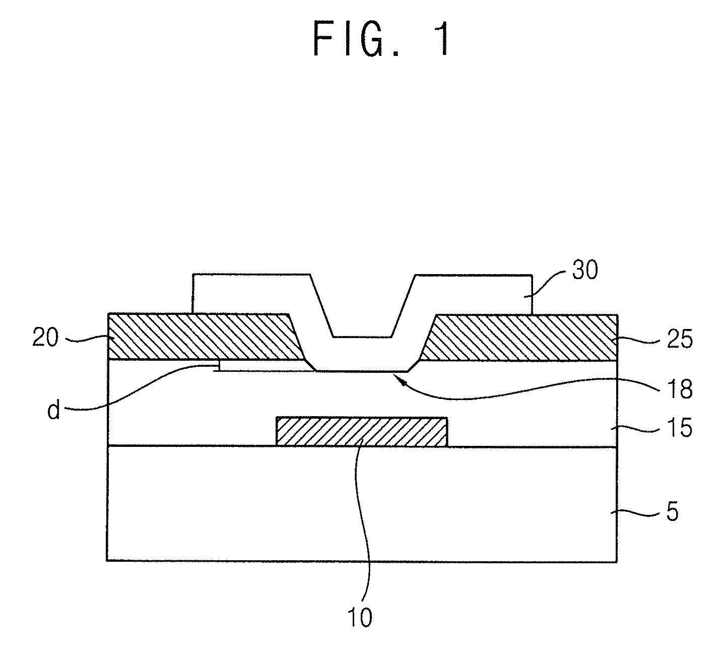
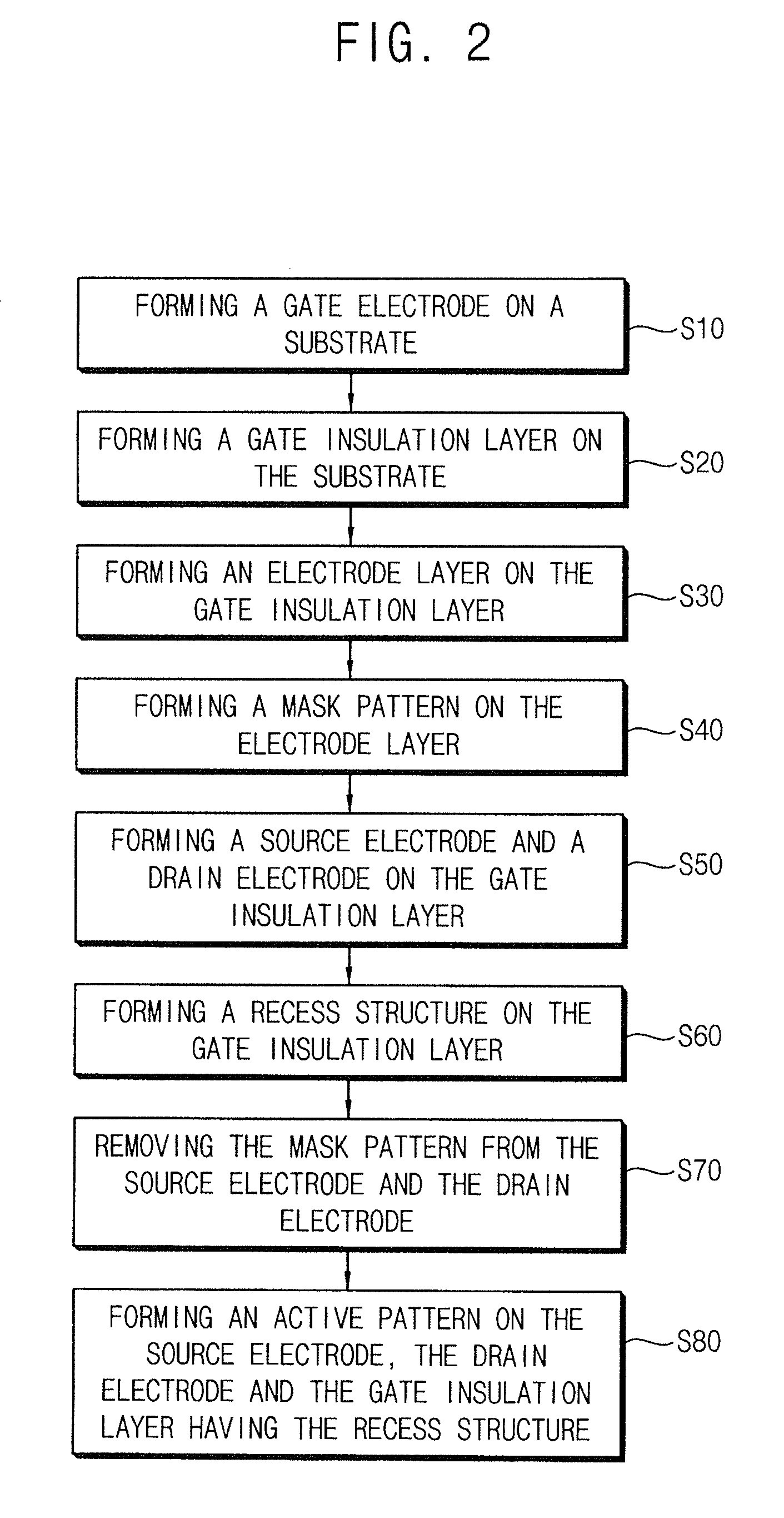
[0169]A gate electrode was formed on a substrate, and then a gate insulation layer was formed on the substrate to cover the gate electrode. After forming an electrode layer on the gate insulation layer, a source electrode and a drain electrode were formed on the gate insulation layer by patterning the electrode layer. A plasma treatment was performed on the gate insulation layer between the source and drain electrodes using a plasma generated from a mixture of sulfur hexafluoride (SF6) and oxygen (O2). A recess structure was formed on the gate insulation layer by the plasma treatment. An active pattern was formed on the gate insulation layer, the source electrode and the drain electrode, thereby obtaining an oxide semiconductor device.

example 2

[0170]A gate electrode was formed on a substrate, and then a gate insulation layer was formed on the substrate to cover the gate electrode. After forming an electrode layer on the gate insulation layer, a source electrode and a drain electrode were formed on the gate insulation layer by patterning the electrode layer. A cleaning treatment was performed on the gate insulation layer between the source and drain electrodes using a solution including hydrogen fluoride. A recess structure was formed on the gate insulation layer by the cleaning treatment. An active pattern was formed on the gate insulation layer, the source electrode and the drain electrode, so that an oxide semiconductor device was provided on the substrate.

example 3

[0171]After gate electrode formed on a substrate, a gate insulation layer was formed on the substrate to cover the gate electrode. After forming an electrode layer on the gate insulation layer, a source electrode and a drain electrode were formed on the gate insulation layer by patterning the electrode layer. A plasma treatment was primarily performed on the gate insulation layer between the source and drain electrodes using a plasma generated from a mixture of sulfur hexafluoride and oxygen. Then, a cleaning treatment was performed on the gate insulation layer using a solution including hydrogen fluoride. A recess structure was formed on the gate insulation layer by the plasma treatment and the cleaning treatment. An active pattern was formed on the gate insulation layer, the source electrode and the drain electrode, thereby obtaining an oxide semiconductor device.


PUM


Abstract

An oxide semiconductor device includes a gate electrode on a substrate, a gate insulation layer on the substrate, the gate insulation layer having a recess structure over the gate electrode, a source electrode on a first portion of the gate insulation layer, a drain electrode on a second portion of the gate insulation layer, and an active pattern on the source electrode and the drain electrode, the active pattern filling the recess structure.

Description

CROSS-REFERENCE TO RELATED APPLICATION[0001]This application claims priority under 35 USC §119 to Korean Patent Application No. 2011-46116 filed on May 17, 2011 in the Korean Intellectual Property Office (KIPO), the contents of which are herein incorporated by reference in their entirety.BACKGROUND[0002]1. Field[0003]Embodiment of the present invention relate to oxide semiconductor devices, methods of manufacturing oxide semiconductor devices, display devices having oxide semiconductor devices, and methods of manufacturing display devices including oxide semiconductor devices. More particularly, embodiments relate to oxide semiconductor devices including gate insulation layers having recess structures, methods of manufacturing the oxide semiconductor devices including the gate insulation layers having the recess structures, display devices including the oxide semiconductor devices, and methods of manufacturing display devices having the oxide semiconductor devices.[0004]2. Descripti...

Claims


Application Information

Patent Timeline
Patent Type & Authority Applications(United States)
IPC IPC(8): H01L27/15H01L21/36H01L33/00H01L29/786
CPCH01L29/42384H01L29/66969H01L29/7869H01L27/1225H01L29/66742H01L29/4908H01L29/78696H01L21/0206H01L29/78618H01L21/32136H10K59/1201H01L21/44H01L21/467H01L21/477H01L27/1259
Inventor WANG, SEONG-MINAHN, KI-WANYOON, JOO-SUNKIM, KI-HONG
Owner SAMSUNG DISPLAY CO LTD
Why Eureka
Try Eureka