Electrophoretic display device and method for manufacturing thereof

An electrophoretic display and gate electrode technology, which is applied to identification devices, circuits, electrical components, etc., can solve the problems of reduced yield, high cost, complex semiconductor film processes, etc., and achieves light weight, high electrical characteristics, and high reliability. Effect

Inactive Publication Date: 2009-03-25
SEMICON ENERGY LAB CO LTD
View PDF3 Cites 21 Cited by
  • Summary
  • Abstract
  • Description
  • Claims
  • Application Information

AI Technical Summary

Problems solved by technology

However, compared with the use of an amorphous semiconductor film, when a polycrystalline semiconductor film is used, the process for crystallizing the semiconductor film is complicated, resulting in a decrease in yield and high cost.

Method used


Image

  • Electrophoretic display device and method for manufacturing thereof
  • Electrophoretic display device and method for manufacturing thereof
  • Electrophoretic display device and method for manufacturing thereof

Examples


Embodiment approach 1

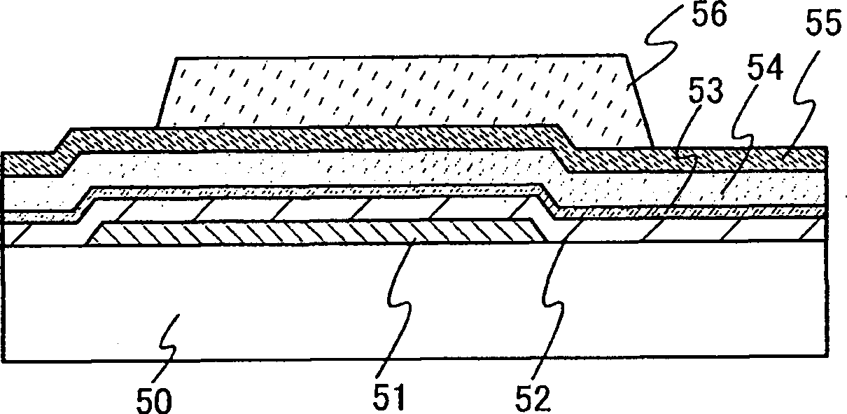
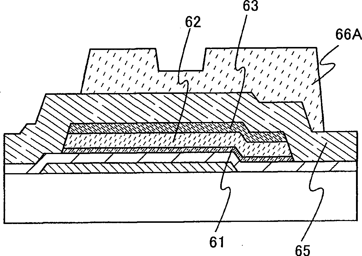
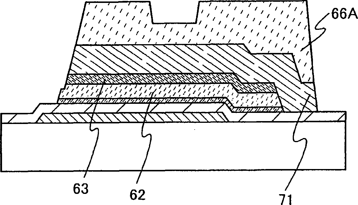
[0033] In this embodiment, refer to Figure 1A to Figure 6C The manufacturing process of an electrophoretic display device, especially the manufacturing process of a pixel having a thin film transistor will be described. Figure 1A to Figure 3B is a cross-sectional view showing a manufacturing process of a thin film transistor, Figure 4 It is a figure explaining the electrophoretic display element, Figure 5A to Figure 5B It is a plan view and its vertical cross-sectional view showing a connection region of a thin film transistor and a pixel electrode in a pixel. FIG. 6 is a diagram showing the appearance of an electrophoretic display device.

[0034] An n-channel type thin film transistor having a microcrystalline semiconductor film is more preferably used for a driving circuit because its mobility is higher than that of a p-channel type thin film transistor having a microcrystalline semiconductor film. It is preferable to make the polarity of all the thin film transistor...

Embodiment approach 2

[0094] In this embodiment mode, manufacturing processes different from those of the electrophoretic display device shown in Embodiment Mode 1 will be described with reference to FIGS. 7A to 8B .

[0095] First, a molybdenum film 702 is formed on a support substrate 701 . A glass substrate, a ceramic substrate, or a quartz substrate can be used as the supporting substrate 701 . In this embodiment mode, a glass substrate is used. In addition, as the molybdenum film 702, a molybdenum film of 30 nm to 200 nm formed by a sputtering method is used. Since the substrate sometimes needs to be fixed in the sputtering method, thickness unevenness of the molybdenum film near the edge of the substrate tends to occur. Therefore, it is preferable to remove the molybdenum film near the edge by dry etching.

[0096] Next, the surface of the molybdenum film 702 is oxidized to form a molybdenum oxide film 703 . As a method for forming the molybdenum oxide film 703, the surface of the molybde...

Embodiment approach 3

[0111] In this embodiment mode, the appearance and cross section of the electrophoretic display device of the present invention will be described with reference to FIGS. 9A and 9B . 9A and 9B are diagrams of an electrophoretic display device in which a thin film transistor 4010 having a microcrystalline semiconductor film formed on a first flexible substrate 4001 and an electrophoretic display element are sealed with a sealing material 4005 between the second flexible substrate 4006. 4008. Fig. 9B corresponds to a cross-sectional view along line A-A' of Fig. 9A.

[0112] A sealing material 4005 is provided to surround the pixel portion 4002 and the scanning line driver circuit 4004 formed on the first flexible substrate 4001 . In addition, a second flexible substrate 4006 is provided on the pixel portion 4002 and the scanning line driver circuit 4004 . Therefore, the pixel portion 4002 and the scanning line driver circuit 4004 are sealed together with the electrophoretic dis...


PUM

PropertyMeasurementUnit
particle diameteraaaaaaaaaa
band gapaaaaaaaaaa
band gapaaaaaaaaaa

Abstract

It is an object to provide an electrophoretic display device having a thin film transistor which has highly reliable electric characteristics, lightweight, and flexibility. A gate insulating film is formed over a gate electrode, a microcrystalline semiconductor film which functions as a channel formation region is formed over the gate insulating film, a buffer layer is formed over the microcrystalline semiconductor film, a pair of source and drain regions are formed over the buffer layer, a pair of the source and drain electrodes in contact with the source and drain regions are formed. Then, the inverted-staggered thin film transistor is interposed between the flexible substrates, and the thin film transistor is provided with electrophoretic display element which is electrically connectedby the pixel electrode. Then, the electrophoretic display electrode is surrounded by the partition layer so as to cover the end portion of the pixel electrode and provided over the pixel electrode.

Description

technical field [0001] The present invention relates to a display device having an electrophoretic display element and a method for manufacturing the same. Among them, the electrophoretic display element is an element in which an image is displayed by changing emissivity by applying a voltage to electrodes sandwiching microparticles dispersed in a solvent to move or rotate the microparticles. In particular, the present invention relates to an electrophoretic display device formed by combining a thin film transistor (hereinafter referred to as TFT) in which a channel region is formed using a microcrystalline semiconductor, and an electrophoretic display element, and a method for manufacturing the same. Background technique [0002] In recent years, electronic paper (also referred to as digital paper or paper-like display) has attracted attention, and a part thereof has been put into practical use. The final target shape of electronic paper is as follows: it is as thin as pap...

Claims


Application Information

Patent Timeline
Patent Type & Authority Applications(China)
IPC IPC(8): G02F1/167G09F9/37G02F1/16755G02F1/16757G02F1/1679
CPCH01L29/78696H01L29/78603G02F1/1368H01L27/1214G02F1/167H01L27/1266H01L29/04H01L29/78678H01L29/78669H01L27/1218G02F1/1679G02F1/16757G02F1/16755
Inventor 山崎舜平
Owner SEMICON ENERGY LAB CO LTD
Why Eureka
Try Eureka