Semiconductor device and semiconductor device manufacturing method

Active Publication Date: 2014-03-13
FUJI ELECTRIC CO LTD
View PDF3 Cites 21 Cited by
  • Summary
  • Abstract
  • Description
  • Claims
  • Application Information

AI Technical Summary

Benefits of technology

[0056]According to the invention, by the end portion form of the mask dielectric (oxide film) of the light element irradiation for introducing the point defects being a tapered form that widens from the upper surface side to the n− type drift layer side, it is possible to change the amount of platinum taken into the mask dielectric in accordance with the thickness of the tapered portion of the mask dielectric. Because of this, it is possible to control the curvature radius of the end portion of the p-type inversion enhancement region. Also, it is possible to change the penetration depth of the light element irradiation from the n− type drift layer surface side using the tapered portion of the mask dielectric. Because of this, it is possible to form the point defect region with a desired point defect density distribution, and with good controllability.
[0057]Also, according to the invention, by platinum being introduced into the region in which the point defect region has been introduced, the formation of the platinum into an acceptor is advanced by the point defect region, and it is possible to form the p-type inversion enhancement region formed by the platinum being formed into an acceptor in accordance with the point defect density distribution of the point defect region. Because of this, by controlling the point defect density distribution of the point defect region, it is possible to control the depth of the p-type inversion enhancement region. Because of this, when utilizing the p-type inversion enhancement region as an anode region, it is possible to form a p-n junction portion of the anode region and a drift layer to a predetermined junction depth, stably and with good controllability.
[0058]Also, acc

Problems solved by technology

In JP-A-2002-231968 and JP-A-2012-38810, it is possible to form a p-n junction portion of a p-type inversion region and an n− type drift layer in the vicinity of a surface of the n− type drift layer by platinum diffusion, and in JP-A-2012-38810 it is possible to improve the stability of forming the p-type inversion region by platinum diffusion by the introduction of point defects, but it is not possible to greatly change the platinum diffusion itself in the n− type drift layer.
However, the donor concentration other than in the vicinity of the surface of the n− type drift layer is also compensated by the platinum acceptor, and a problem occurs in that the lifetime of the whole of the n− type drift layer decreases, and the on-state voltage (forward voltage VF) increases.
Also, when reducing the donor concentration of the n− type drift layer, a problem occurs in that reverse surge withstand capability decreases, and the like.
Also, it is unrealistic in terms of diode manufacture to reduce the donor concentration by as large an extent to which the compensation by the platinum acceptor changes.
However, when the element characteristics are adversely affected by damage (wire bonding damage) received from the chip surface when assembling or by impurities or moisture diffused from the chip surface, there is a demand for the device characteristics to be stabilized by the p-n junction portion of the p-type inversion region and n− type drift layer being a deep junction.
As a

Method used


Image

  • Semiconductor device and semiconductor device manufacturing method
  • Semiconductor device and semiconductor device manufacturing method
  • Semiconductor device and semiconductor device manufacturing method

Examples


embodiment 1

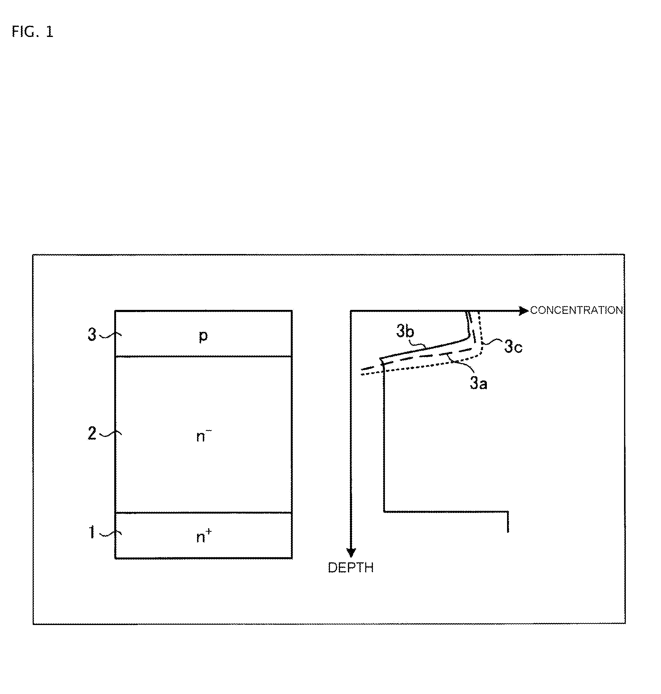
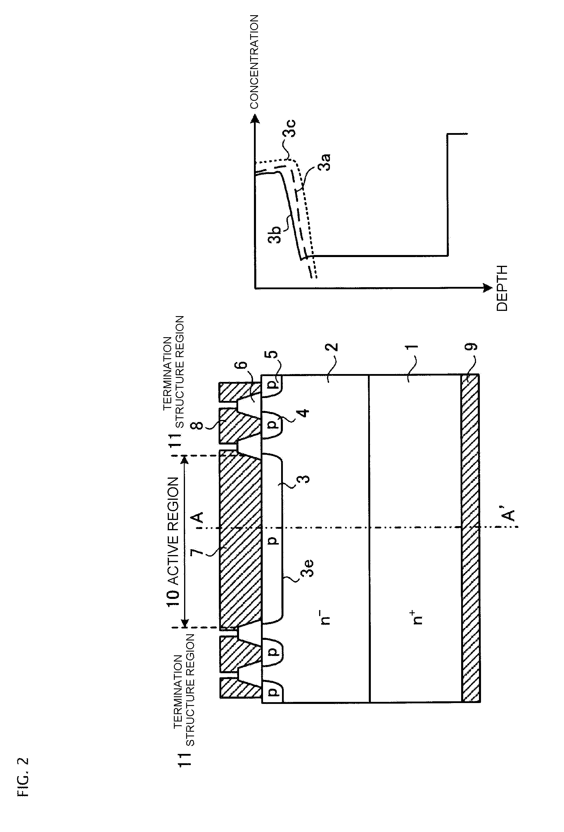
[0105]Next, a description will be given of the structure of a semiconductor device according to Embodiment 1. FIG. 2 is a sectional view showing the configuration of the semiconductor device according to Embodiment 1. FIG. 2 shows the sectional structure of the semiconductor device according to Embodiment 1, and the impurity concentration distribution in the depth direction. The semiconductor device according to Embodiment 1 shown in FIG. 2 is a diode wherein p-type guard ring region (second inversion region) 4 and p-type channel stopper region 5 of a termination structure region 11 are provided in the basic structure of the diode shown in FIG. 1.

[0106]Termination structure region 11, being a region from an end portion of active region 10 to an outer peripheral end portion of the semiconductor substrate (semiconductor chip), is a structural portion that encloses active region 10, and alleviates the electrical field intensity of the semiconductor substrate front surface (the surface ...

embodiment 2

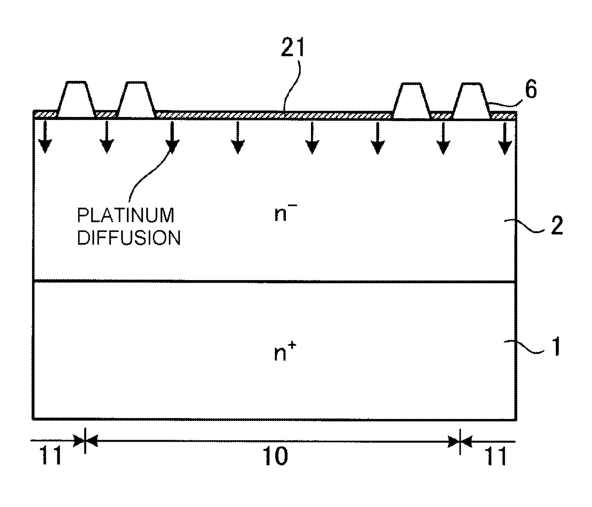
[0115]Next, a description will be given of a method of manufacturing the semiconductor device according to Embodiment 1 as a semiconductor device manufacturing method according to Embodiment 2. FIGS. 3 to 6 are sectional views showing conditions partway through the manufacture of the semiconductor device according to Embodiment 2. For example, the description will be given taking the rated voltage to be 1,000V and the transition metal used in the formation of p-type inversion enhancement region 3b to be platinum (the same also applies in other Embodiments 3 and 5). Firstly, n− type drift layer 2 with a thickness of, for example, 100 μm is epitaxially grown with a resistivity of 60 Ωcm on n+ type semiconductor substrate 1 forming an n+ type cathode layer.

[0116]Next, oxide film 6 with a thickness of, for example, 900 nm is formed using thermal oxidation on the surface of n− type drift layer 2. The thickness of oxide film 6 is arbitrarily determined in accordance with the dose and pene...

embodiment 3

[0125]Next, a description will be given of a semiconductor device manufacturing method according to Embodiment 3. FIGS. 7 and 8 are sectional views showing conditions partway through the manufacture of the semiconductor device according to Embodiment 3. The semiconductor device manufacturing method according to Embodiment 3 differs from the semiconductor device manufacturing method according to Embodiment 2 in that the process order of the proton irradiation and platinum diffusion is changed, so that the platinum diffusion is carried out before the proton irradiation. Specifically, the processes of the semiconductor device manufacturing method according to Embodiment 3 are carried out as follows.

[0126]Firstly, in the same way as in Embodiment 2, oxide film 6 and phosphorus silicon glass are formed sequentially on the surface of n− type drift layer 2 deposited on n+ type semiconductor substrate 1, after which plasma treatment is carried out on oxide film 6 surface (FIG. 3). Next, in ...


PUM


Abstract

A simplified manufacturing process stably produces a semiconductor device with high electrical characteristics, wherein platinum acts as an acceptor. Plasma treatment damages the surface of an oxide film formed on a ntype drift layer deposited on an n+ type semiconductor substrate. The oxide film is patterned to have tapered ends. Two proton irradiations are carried out on the ntype drift layer with the oxide film as a mask to form a point defect region in the vicinity of the surface of the ntype drift layer. Silica paste containing 1% by weight platinum is applied to an exposed region of the ntype drift layer surface not covered with the oxide film. Heat treatment inverts the vicinity of the surface of the ntype drift layer to p-type by platinum atoms which are acceptors. A p-type inversion enhancement region forms a p-type anode region.

Description

BACKGROUND OF THE INVENTION[0001]A. Field of the Invention[0002]The present invention relates to a semiconductor device and semiconductor device manufacturing method.[0003]B. Description of the Related Art[0004]Rectifier diodes utilizing a silicon (Si) semiconductor p-n junction are known. In particular, high speed recovery diodes in which reverse recovery time is improved are widely used in high frequency switching applications. A diode is configured of a p-type anode layer, an n+ type cathode layer, and an n− type drift layer provided between the p-type anode layer and n+ type cathode layer in order to maintain high breakdown voltage, and exhibits rectifying characteristics using a p-n junction of the p-type anode layer and n− type drift layer.[0005]As the n− type drift layer has an impurity concentration lower than that of the p-type anode layer or n+ type cathode layer, it is also called an i-type layer (intrinsic region). As impurities introduced into each silicon layer configu...

Claims


Application Information

Patent Timeline
IPC IPC(8): H01L29/36H01L21/22
CPCH01L21/22H01L29/36H01L21/221H01L21/263H01L29/66204H01L29/66136H01L29/861H01L21/3105H01L21/31111H01L21/225H01L29/063H01L29/6609H01L29/868
Inventor KITAMURA, SHOJI
Owner FUJI ELECTRIC CO LTD
Why Eureka
Try Eureka