Semiconductor device and semiconductor device manufacturing method

a semiconductor device and manufacturing method technology, applied in the direction of semiconductor devices, electrical devices, transistors, etc., can solve the problems of reverse breakdown voltage characteristics deterioration, inability to fabricate a low breakdown voltage igbt of a breakdown voltage class of 600v, and inability to reduce the thickness of the wafer below 200/b>, so as to reduce the thickness of the chip, reduce the concentration of stress on the wafer, and facilitate maintenance

Inactive Publication Date: 2015-03-05
FUJI ELECTRIC CO LTD
View PDF15 Cites 20 Cited by
  • Summary
  • Abstract
  • Description
  • Claims
  • Application Information

AI Technical Summary

Benefits of technology

[0048]According to embodiments of the invention, it is possible to disperse the concentration of stress on the wafer by the thickness of the chip outer peripheral portion being left greater than the thickness of the chip inner portion in each region on the wafer that forms a chip. Also, by the thickness of the chip outer peripheral portion being left greater than the thickness of the chip inner portion, and the distance in the chip thickness direction between the collector electrode and a field stop region being greater in most of the edge termination structure portion than in the active region, it is possible to reduce the amount of carriers injected from the collector region in the edge termination structure portion compared with a semiconductor device wherein the chip thickness is uniform from the edge termination structure portion to the active region. Because of this, the possibility of the edge termination structure portion being destroyed when a large current is turned off is markedly reduced, and the reverse biased safe operating area (RBSOA) of the element becomes easier to maintain.
[0049]Also, according to embodiments of the invention, by a groove being formed in the back surface of the wafer, leaving the thickness of the chip outer peripheral portion greater than the thickness of the chip inner portion in each region that forms a chip, it is possible to reduce the chip thickness in the active region compared with that in a heretofore known rib wafer wherein only the wafer outer peripheral portion is left thicker than the wafer central portion. Also, by a deep groove reaching the field stop region being formed from the back surface of the wafer, it is possible to further reduce the thickness of the chip inner portion. Because of this, when fabricating a low breakdown voltage IGBT of a breakdown voltage class of, for example, 600V or less, it is possible for the thickness of the drift region to be the ideal thickness demanded by the design in order to realize the required breakdown voltage.
[0050]Also, according to embodiments of the invention, by the thickness of the chip outer peripheral portion being left greater than the thickness of the chip inner portion in each region that forms a chip, the collector region, the collector electrode, and the like, provided in the active region do not come into contact with a support stand on which the wafer is mounted during, for example, an electrical characteristic test carried out on the wafer before dicing. Because of this, it is possible to prevent the occurrence of a problem wherein the collector region or the field stop region is damaged, and the voltage drops and leakage current increases, and of a problem wherein the collector region is damaged, and the reverse breakdown voltage characteristics degrade or the reverse breakdown voltage characteristics become unobtainable.
[0051]According to the semiconductor device and semiconductor device manufacturing method according to embodiments of the invention, an advantage is obtained in that it is possible to increase the mechanical strength. Also, according to the semiconductor device and semiconductor device manufacturing method according to embodiments of the invention, an advantage is obtained in that it is possible to provide a semiconductor device and semiconductor device manufacturing method having optimum electrical characteristics.

Problems solved by technology

However, as it is not possible when considering manufacturability for the wafer thickness to be the limit thickness or lower, the thickness of the n− type drift region 102 of an IGBT of a breakdown voltage class of 600V or less is generally 60 μm or more, which is the ideal thickness.
Consequently, it is not possible for the thickness of the wafer 200 to be reduced below 80 μm, which is the limit thickness at which no problem occurs in terms of manufacturability, and thus not possible to fabricate a low breakdown voltage IGBT of a breakdown voltage class of 600V or less under ideal design conditions.
Also, the heretofore known RB-IGBT is such that there is concern that the p-type collector region 111 will be damaged by extraneous matter or friction occurring on the back surface of the wafer 200, and that the reverse breakdown voltage characteristics will deteriorate or the reverse breakdown voltage characteristics will become unobtainable.

Method used


Image

  • Semiconductor device and semiconductor device manufacturing method
  • Semiconductor device and semiconductor device manufacturing method
  • Semiconductor device and semiconductor device manufacturing method

Examples


embodiment 1

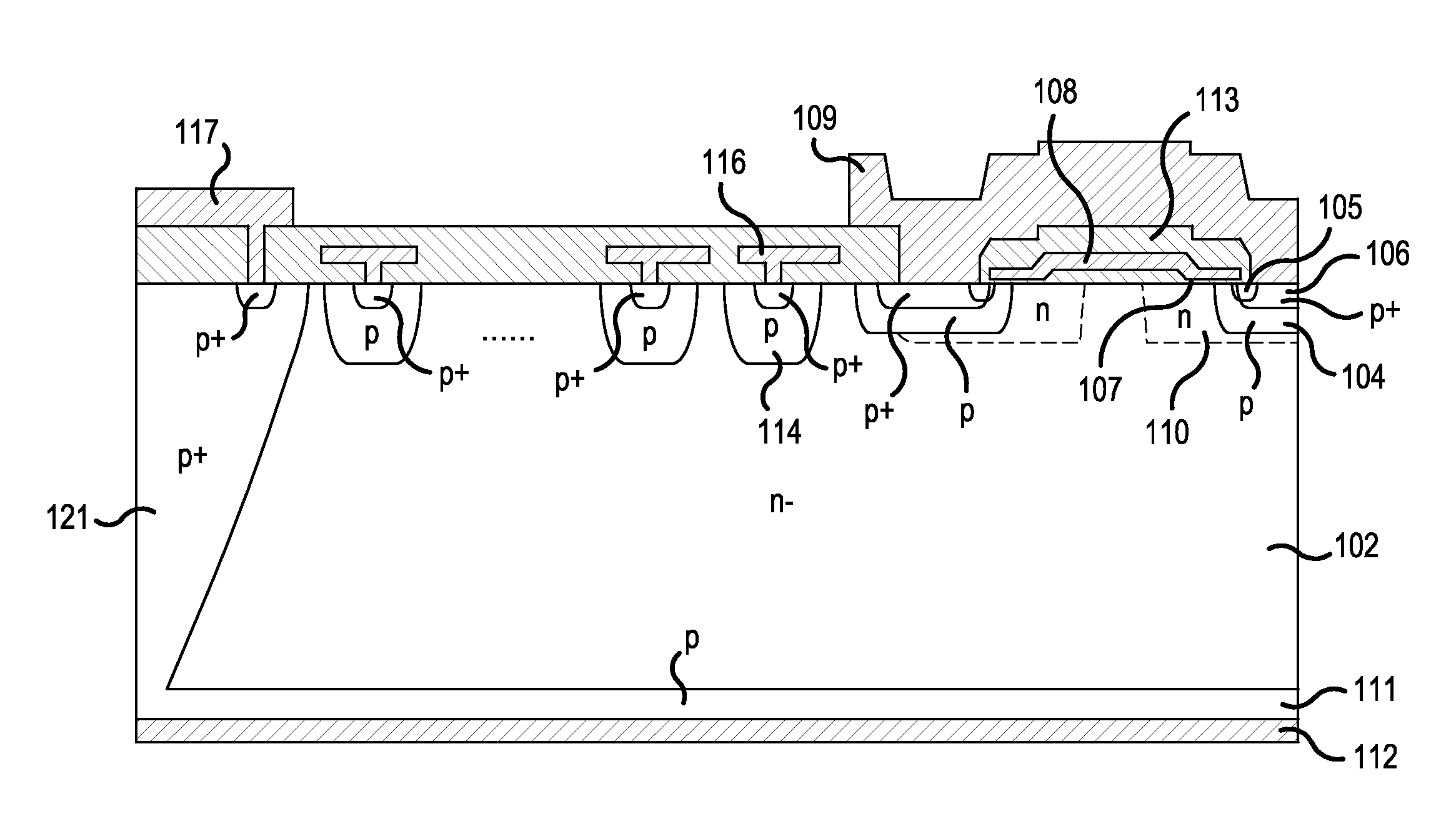
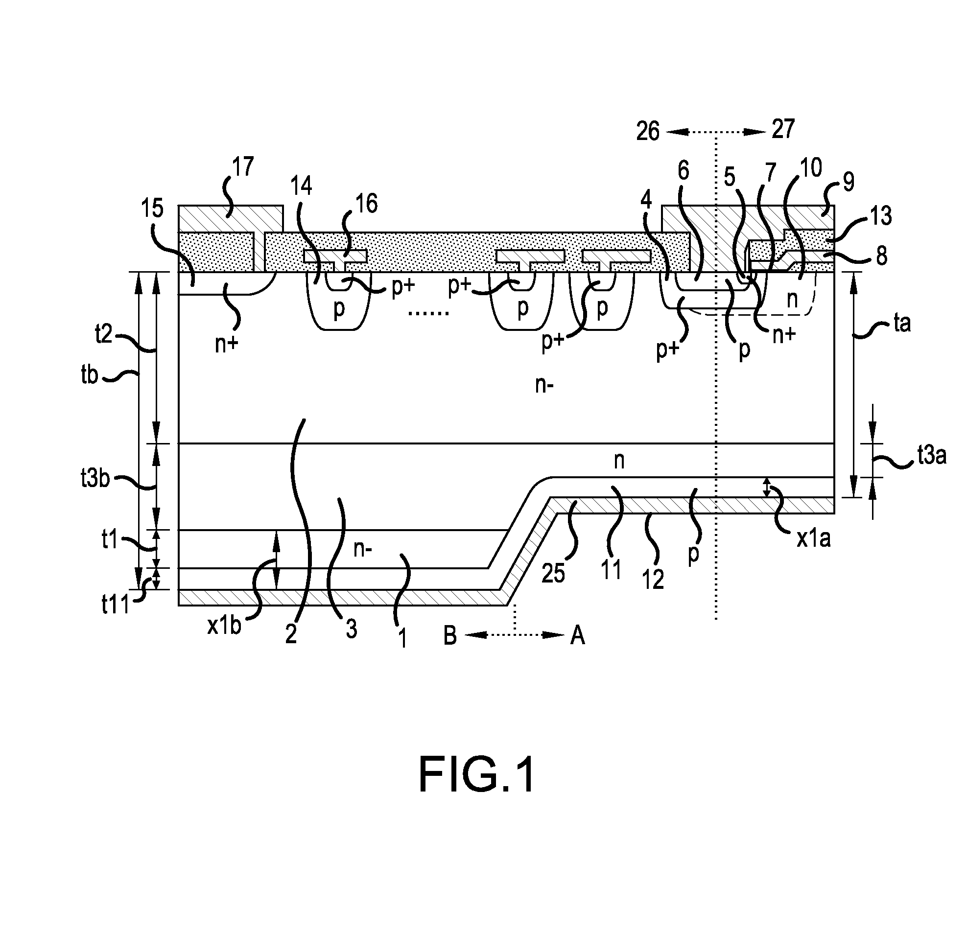
[0085]A description will be given of a configuration of a semiconductor device according to Embodiment 1, with a planar gate structure field stop IGBT (FS-IGBT) shown in FIG. 1 as an example. FIG. 1 is a cross sectional diagram showing a configuration of the semiconductor device according to Embodiment 1. As shown in FIG. 1, the semiconductor device according to Embodiment 1 includes, on an n− type wafer, an edge termination structure portion 26 that relaxes an electrical field exerted on an n− type drift region 2, thus maintaining breakdown voltage, and an active region 27 through which current flows when the semiconductor device is in an on-state.

[0086]The n− type wafer is formed by, for example, an n− type FZ wafer (first first conductivity type semiconductor region) 1, an n-type field stop region (third first conductivity type semiconductor region) 3, and an n− type drift region (second first conductivity type semiconductor region) 2 being deposited sequentially from the back su...

embodiment 2

[0116]A description will be given of a semiconductor device according to Embodiment 2. FIG. 12 is a cross sectional diagram showing a configuration of the semiconductor device according to Embodiment 2. The semiconductor device according to Embodiment 2 differs from the semiconductor device according to Embodiment 1 in that a groove 35 provided in the back surface of the n− type wafer is designed so as not to reach the n-type field stop region 3. That is, the p-type collector region 11 is in contact with only the n− type FZ wafer 1 from the edge termination structure portion 26 to the active region 27.

[0117]A third distance x2a in the chip thickness direction between the p-type collector region 11 and n-type field stop region 3 in the chip inner portion A is less than a fourth distance x2b in the chip thickness direction between the p-type collector region 11 and the n-type field stop region 3 in the chip outer peripheral portion B. The third distance x2a may be an arbitrary thickne...

embodiment 3

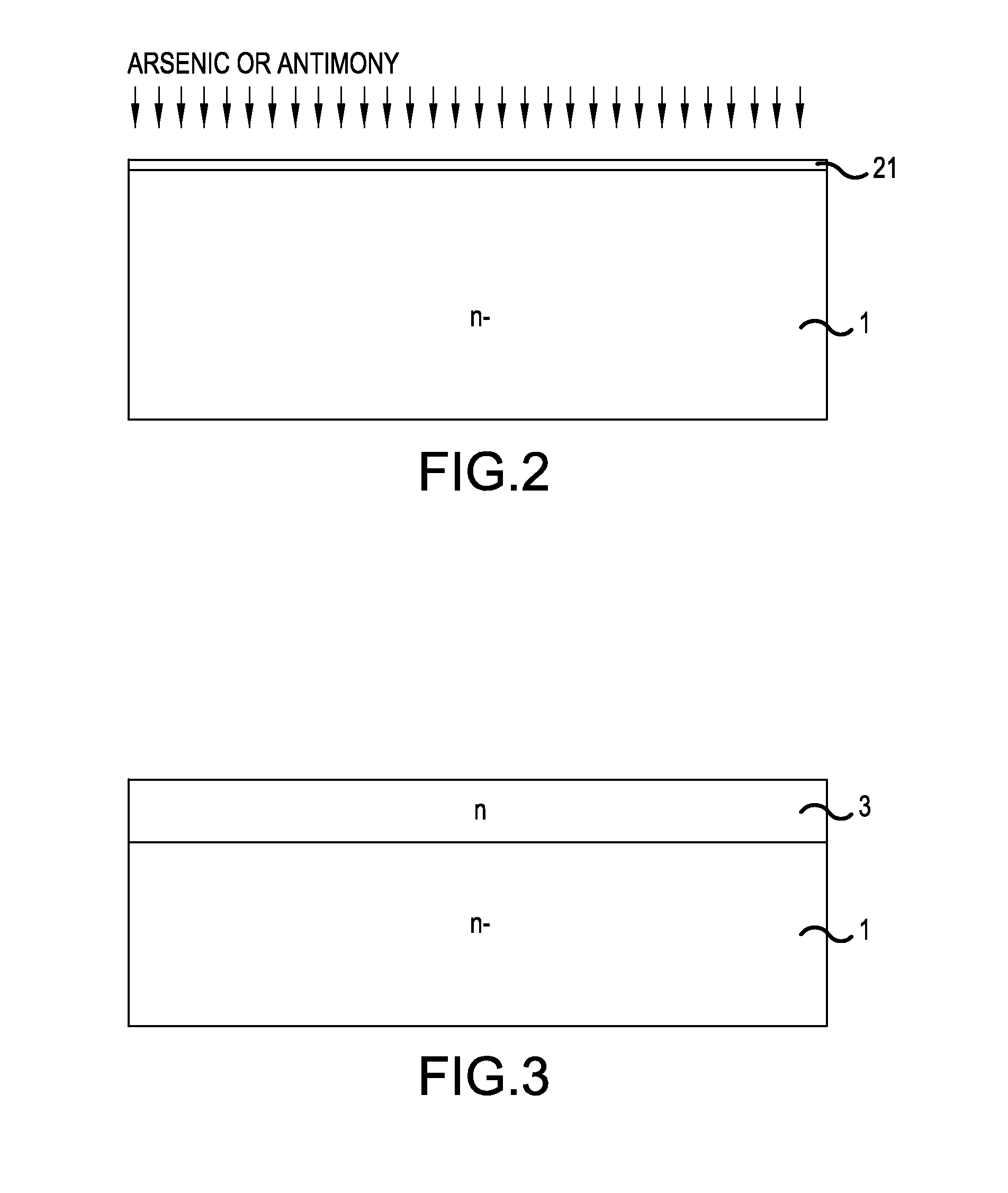
[0123]Next, a description will be given of a semiconductor device manufacturing method according to Embodiment 3, with an example case of fabricating a 400V breakdown voltage class FS-IGBT. FIGS. 15 and 16 are cross sectional diagrams showing states partway through the manufacture of the semiconductor device according to Embodiment 3. The semiconductor device manufacturing method according to Embodiment 3 differs from the semiconductor device manufacturing method according to Embodiment 1 in that an n− type FZ wafer 41 thicker than that of Embodiment 1 is used, and that the n-type field stop region 3 is formed using a proton (H+) implantation 43 and a thermal annealing process for transforming the protons into donors.

[0124]Specifically, firstly, for example, the n− type FZ wafer 41, of a thickness greater than the thickness tb of the chip outer peripheral portion B after completion of the FS-IGBT, is prepared, as shown in FIG. 15. Specifically, the thickness of the n− type FZ wafer ...


PUM


Abstract

An n type drift region, an n-type field stop region, and an n type FZ wafer are provided in an n type wafer. An edge termination structure portion is provided in a chip outer peripheral portion of regions of the n type wafer, surrounding an active region inside a chip inner portion. A thickness of the chip inner portion is less than a thickness of the chip outer peripheral portion owing to a groove. A p-type collector region is in contact with the n type FZ wafer and n-type field stop region. A collector electrode is in contact with the p-type collector region. A second distance between the collector electrode and the n-type field stop region in the edge termination structure portion is greater than a first distance between the collector electrode and the n-type field stop region in the active region.

Description

CROSS-REFERENCE TO RELATED APPLICATIONS[0001]This application is a continuation of International Application No. PCT / JP2012 / 073439, filed on Sep. 13, 2012. The disclosure of the PCT application in its entirety, including the drawings, claims, and the specification thereof, is incorporated herein by reference.BACKGROUND[0002]1. Field of the Invention[0003]Embodiments of the present invention relate to a semiconductor device and a semiconductor device manufacturing method.[0004]2. Discussion of the Background[0005]High breakdown voltage discrete power devices play a central role in power conversion equipment. To date, for example, an insulated gate bipolar transistor (IGBT), an insulated gate field effect transistor having a metal-oxide-semiconductor structure (MOSFET: Metal Oxide Semiconductor Field Effect Transistor), and the like, are well known devices suitable as high breakdown voltage discrete power devices in such power conversion equipment.[0006]IGBTs that can reduce on-state ...

Claims


Application Information

Patent Timeline
Patent Type & Authority Applications(United States)
IPC IPC(8): H01L29/739H01L29/66H01L21/306H01L21/265H01L21/324H01L21/304H01L29/06H01L29/36
CPCH01L29/7395H01L29/0619H01L29/66333H01L21/30604H01L21/265H01L21/324H01L21/304H01L29/36H01L21/30608H01L29/0661H01L29/0834H01L29/404H01L21/26506H01L21/268
Inventor LU, HONG-FEI
Owner FUJI ELECTRIC CO LTD
Why Eureka
Try Eureka