Integrated circuit for compression mode scan test

a compression mode and integrated circuit technology, applied in the field of integrated circuits, can solve the problem of not being able to perform the scan test on the device using the compression mode, and achieve the effect of improving the testability and accuracy of the devi

Active Publication Date: 2011-11-24
SAMSUNG ELECTRONICS CO LTD
View PDF11 Cites 13 Cited by
  • Summary
  • Abstract
  • Description
  • Claims
  • Application Information

AI Technical Summary

Benefits of technology

[0007]At least one embodiment of the present invention provides a circuit and method that allows a sc...

Problems solved by technology

However, when integrated circuits manufactured by different companies are interfaced toge...

Method used


Image

  • Integrated circuit for compression mode scan test
  • Integrated circuit for compression mode scan test
  • Integrated circuit for compression mode scan test

Examples


Embodiment Construction

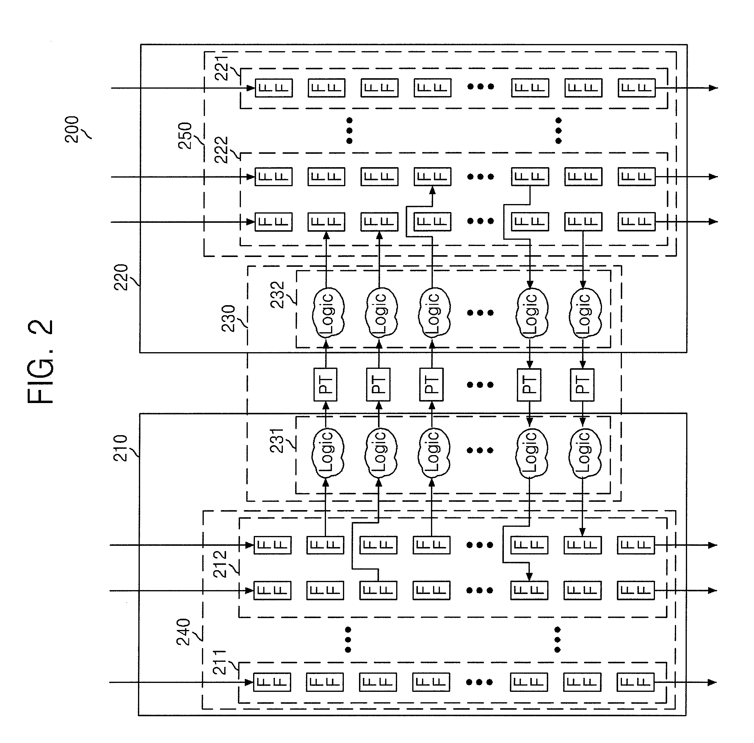
[0034]The present invention now will be described more fully hereinafter with reference to the accompanying drawings, in which exemplary embodiments of the invention are shown. This invention may, however, be embodied in many different forms and should not be construed as limited to the exemplary embodiments set forth herein. In the drawings, the size and relative sizes of layers and regions may be exaggerated for clarity. Like numbers refer to like elements throughout.

[0035]It will be understood that when an element is referred to as being “connected” or “coupled” to another element, it can be directly connected or coupled to the other element or intervening elements may be present.

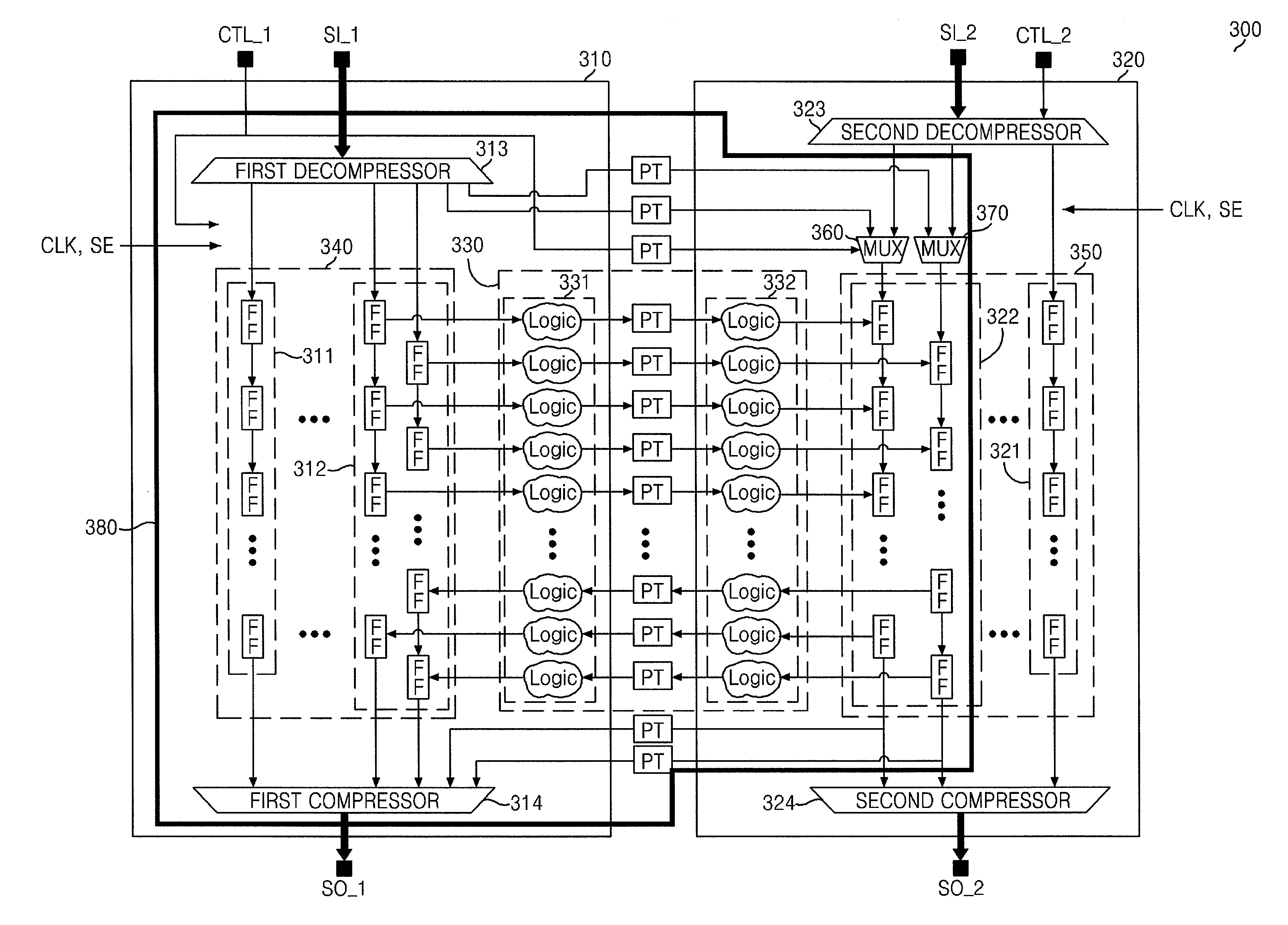
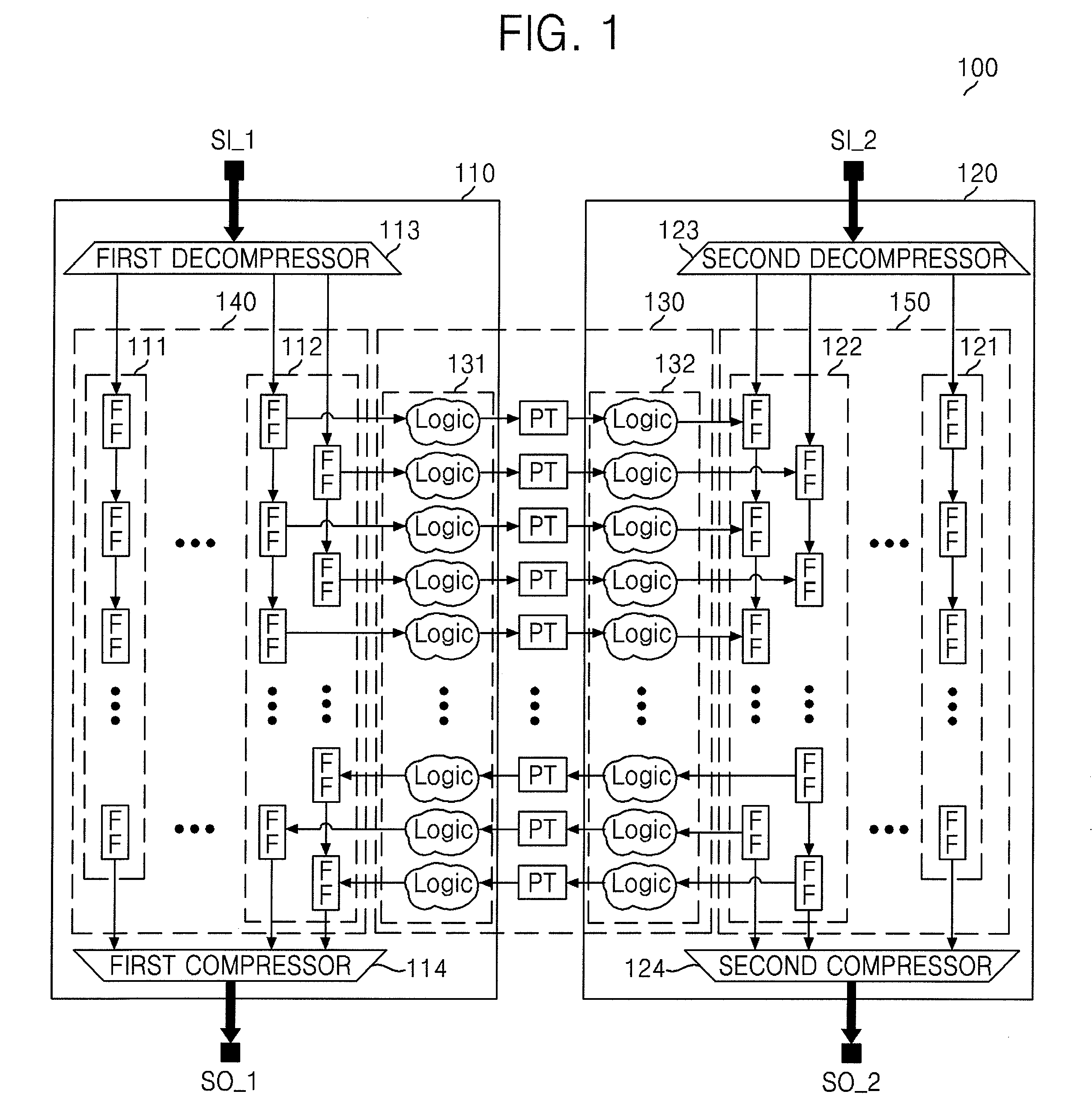
[0036]FIG. 1 is a diagram of an integrated circuit 100 for a compression mode test as a comparison example. The integrated circuit 100 includes a first module 110 and a second module 120.

[0037]The first module 110 includes a first block 140, a first decompressor 113, a first compressor 114, and a first i...


PUM


Abstract

An integrated circuit for performing a design for testability (DFT) scan test is provided. The integrated circuit includes at least one scan chain including a plurality of flip-flops, at least one interface scan chain including a plurality of flip-flops, a decompressor configured to be connected with an input terminal of the at least one interface scan chain and to decompress a first input signal and then transmit it to the at least one scan chain, a compressor configured to be connected with an output terminal of the at least one scan chain and to compress an output signal of the at least one scan chain, and at least one multiplexer configured to be connected with the decompressor and to selectively output an output signal of the decompressor or a second input signal in response to a control signal.

Description

CROSS-REFERENCE TO RELATED APPLICATIONS[0001]This application claims priority under 35 U.S.C. §119(e) to Korean Patent Application No. 10-2010-0046993 filed on May 19, 2010, in the Korean Intellectual Property Office, the disclosure of which is incorporated by reference herein.BACKGROUND[0002]1. Technical Field[0003]Embodiments of the present invention relate to a circuit for performing a design for testability (DFT) scan test, and more particularly, to an integrated circuit for performing a DFT scan test, which can perform different types of DFT scan tests, in a compression mode.[0004]2. Discussion of Related Art[0005]DFT is a name for design techniques that add certain testability features to a microelectronic hardware product design. The premise of the added features is that they make it easier to develop and apply manufacturing tests for the designed hardware. The purpose of manufacturing tests is to validate that the product hardware contains no defects that could, otherwise, a...

Claims


Application Information

Patent Timeline
IPC IPC(8): G01R31/3177G06F11/25
CPCG01R31/318547G01R31/318536G06F11/22
Inventor LEE, HEON-HEELEE, HOI JIN
Owner SAMSUNG ELECTRONICS CO LTD
Why Eureka
Try Eureka