

Thin-Film Piezoelectric Resonator and Thin-Film Piezoelectric Filter Using the Same
- Summary
- Abstract
- Description
- Claims
- Application Information
AI Technical Summary
Benefits of technology
Problems solved by technology
Method used
Image

Examples
example 1
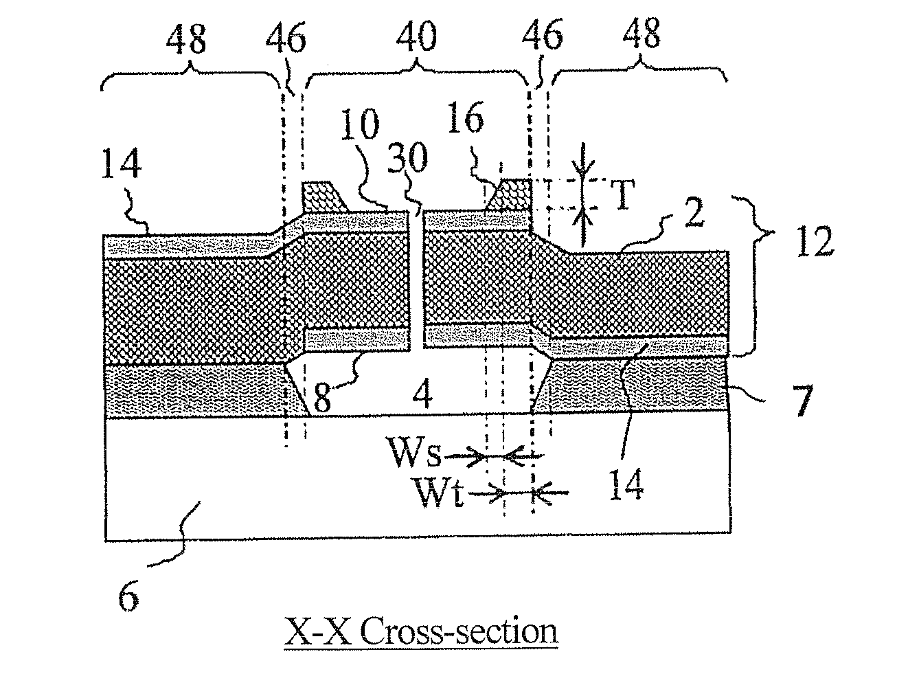
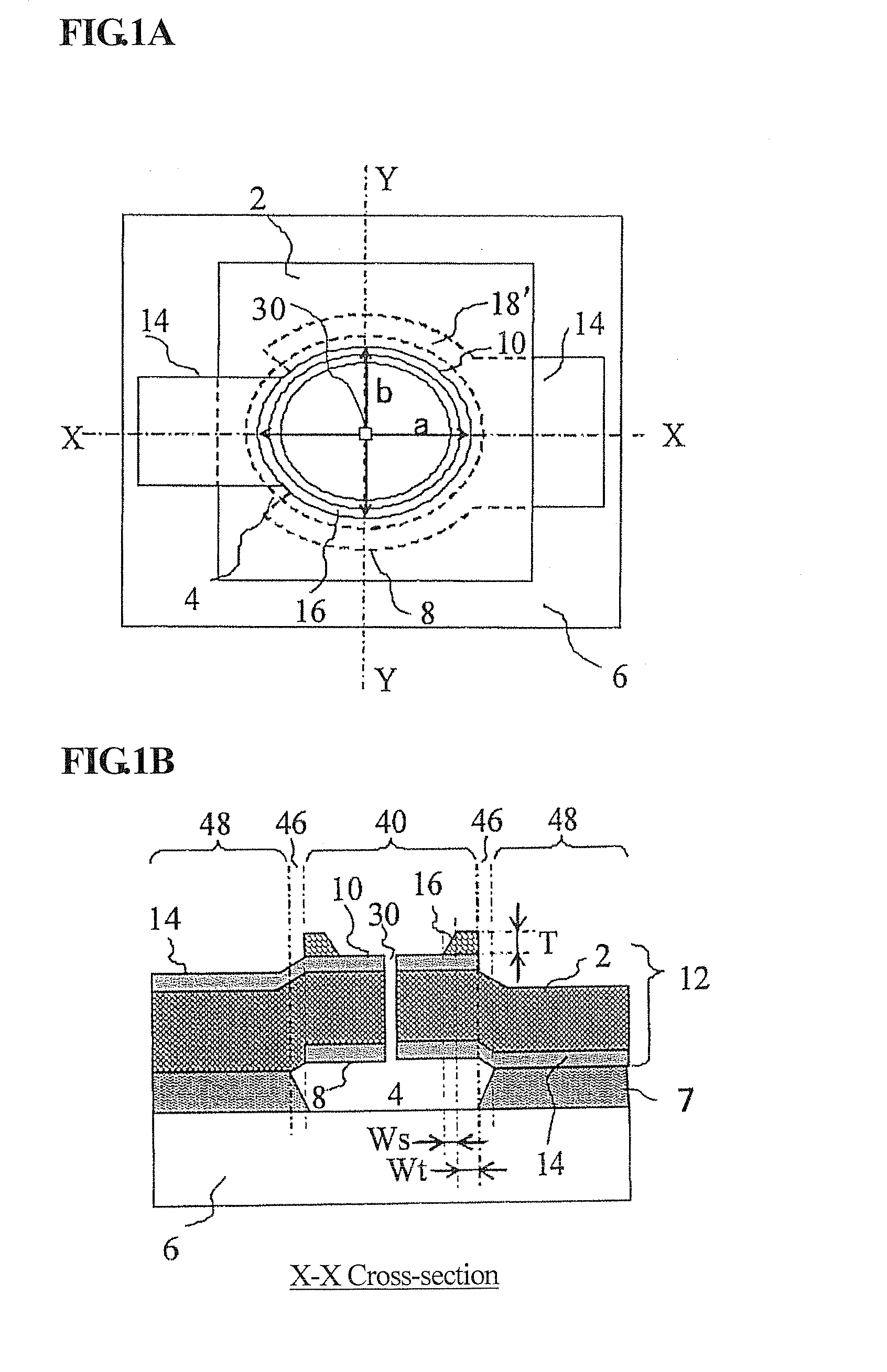
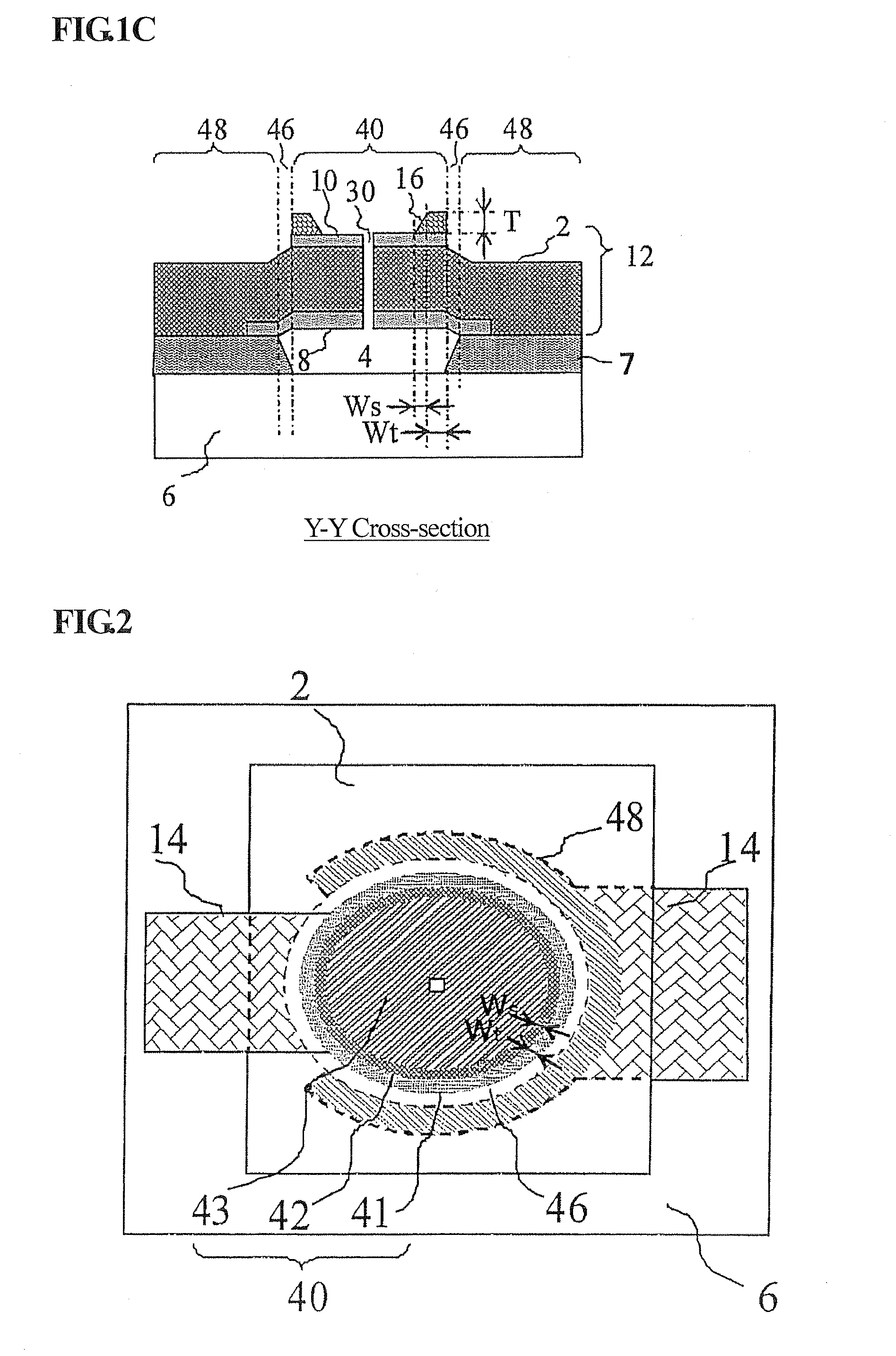
[0156]The thin-film piezoelectric resonator as described in the exemplary embodiment of FIGS. 1A to 1C was produced. The shape of the top electrode 10, i.e., the shape of the vibration region 40 was an ellipse with the major axis dimension a of 107 μm and the minor axis dimension b of 72 μm, and the shape of the through hole 30 was a 5 μm×5 μm square. According to the present example, the material and thickness of each constitutional layer were set as follows: the bottom electrode 8 was made of Mo with a thickness of 300 nm; the piezoelectric layer 2 was made of AlN with a thickness of 1200 nm; and the top electrode 10 was made of Ru with a thickness of 300 nm. Further, the frame layer 16 was made of Mo with a thickness (T) of 100 nm, the first vibration region 41 was formed with a thickness (Wt) of 3 μm, and the second vibration region 42 was formed with a slope angle θ of 20°. In this case, the width (Ws) was 0.27 μm (Ws=T / tan θ).
[0157]The thin-film piezoelectric resonator of Exam...
examples 2 to 5
[0159]The thin-film piezoelectric resonators as described in the exemplary embodiment of FIGS. 1A to 1C were produced in the same manner as Example 1 except that the slope angle θ of the cross-section of the frame layer 16 in the second vibration region 42 was set to 30°, 45°, 60°, or 70°, as illustrated in Table 1. Adjustment of the slope angle θ of the inner peripheral end surface of the frame layer 16 was conducted by adjusting the gas flow rate of the O2 etching gas. In this case, the width (Ws) of the second vibration region 42 was in the range of 0.04 μm to 0.17 μm.
[0160]As illustrated in Table 2, the impedances (Rp) of the obtained thin-film piezoelectric resonators at the antiresonance frequency were as high as 2380Ω to 2740Ω, and Q-values (Qp) were as high as 1420 to 1500. Further, as denoted by the noise level in Table 2, the noise levels in and around the frequency band from the resonance frequency to antiresonance frequency were “low” or “intermediate”. Thus, occurrence ...
examples 6 to 11
[0163]The thin-film piezoelectric resonators as described in the exemplary embodiment of FIGS. 1A to 1C were produced in the same manner as Example 1 except that the width (Wt) of the first vibration region 41 was set to 1.5 μm, 4.0 μm, or 6.0 μm, and slope angle θ of the cross-section of the frame layer 16 in the second vibration region 42 was set to 45° or 60°, as illustrated in Table 1. In this case, the width (Ws) of the second vibration region 42 was 0.10 μm or 0.06 μm.
[0164]As illustrated in Table 2, the impedances (Rp) of the obtained thin-film piezoelectric resonators at the antiresonance frequency were as high as 2220Ω to 2480Ω, and Q-values (Qp) were as high as 1330 to 1430. Further, as denoted by the noise level in Table 2, the noise levels in and around the frequency band from the resonance frequency to antiresonance frequency were “low” or “intermediate”. Thus, occurrence of noise was suppressed.
PUM
 Abstract
Description
Claims
Application Information