

Epitaxial substrate and method for producing same
a technology of epitaxial substrate and substrate, which is applied in the direction of crystal growth process, after-treatment details, transportation and packaging, etc., can solve the problems of increasing the dark current significantly deteriorating the electric properties of the solid-state imaging sensor, and it is difficult to completely avoid metal contamination. , to achieve the effect of reducing the occurrence of white defects of the image sensor, reducing the occurrence of metal contamination, and sufficient gettering capability
Inactive Publication Date: 2011-12-08
SUMCO CORP
View PDF0 Cites 13 Cited by
- Summary
- Abstract
- Description
- Claims
- Application Information
AI Technical Summary
Benefits of technology
[0023]According to the present invention, it is possible to provide an epitaxial substrate and a method for producing the same capable of suppressing metal contamination and thereby reducing occurrence of white defects of an image sensor by maintaining sufficient gettering capability during the device manufacturing process, through a step of growing an epitaxial layer on a silicon substrate containing dopant of carbon to form an epit
Problems solved by technology
However, when a metal is introduced into the epitaxial substrate as an impurity, the introduced metal causes an increase in dark current of an image sensor, posing a problem of significantly deteriorating electric properties of a solid state imaging sensor such as occurrence of a defect called a white defect.
In recent years, these metal contaminations have been improved through replacement of the components of the furnace for epitaxial growth with a component made of a corrosion-resistant material or other efforts, hut it was still difficult to completely avoid the metal contaminations in the process of forming the epitaxial substrate.
On the other hand, in the process of forming the solid state imaging sensor in the latter case, there is a concern about heavy metal contamination
Method used
View moreImage
Smart ImageViewing Examples

Examples
 PUM
 Abstract
[Problem] An object of the present invention is to provide an epitaxial substrate and a method for producing the same capable of suppressing metal contamination and thereby reducing occurrence of white defects of a solid state imaging sensor by maintaining sufficient gettering capability during a device manufacturing process.
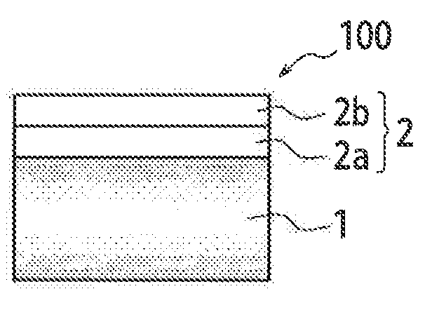
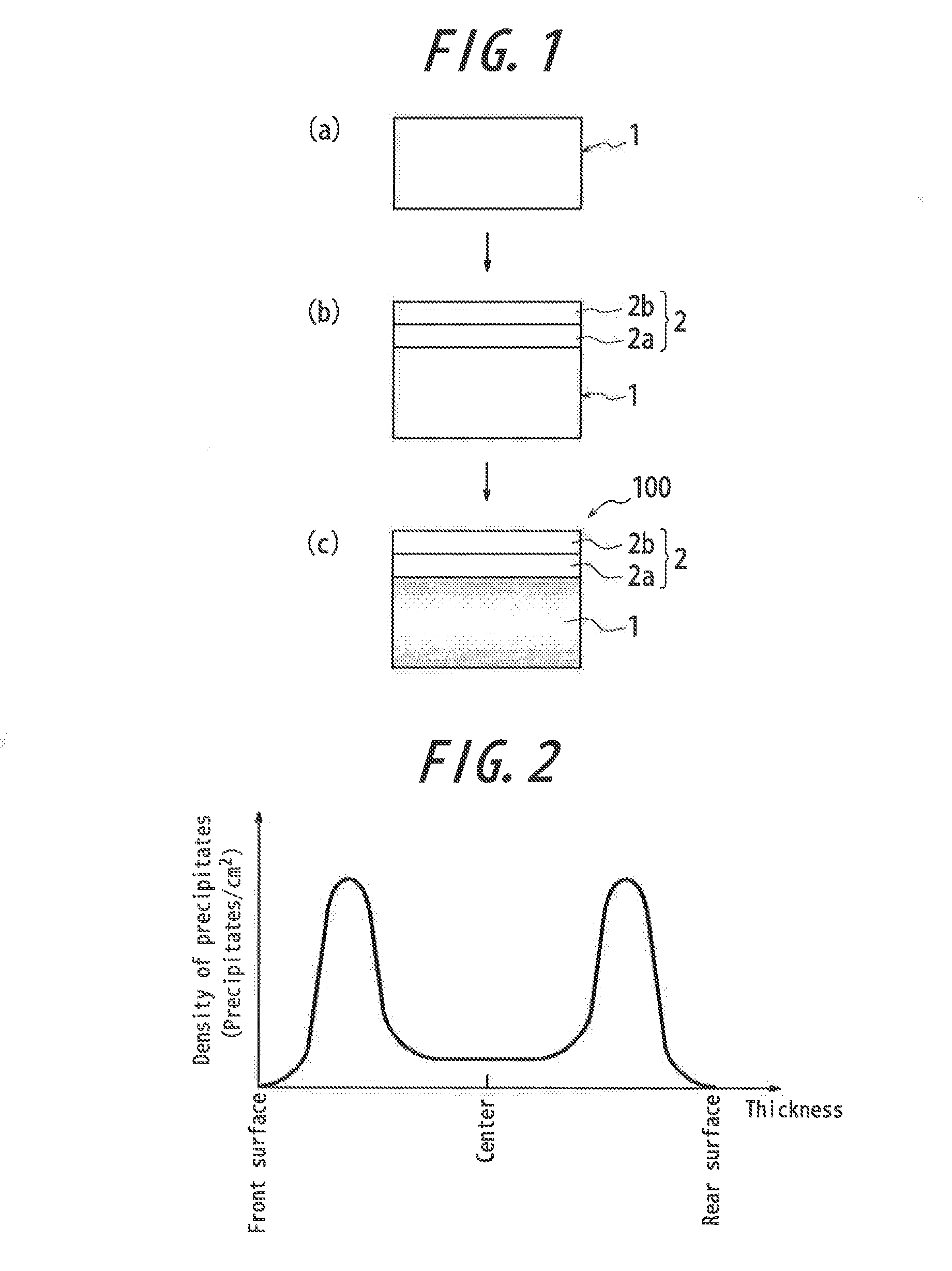
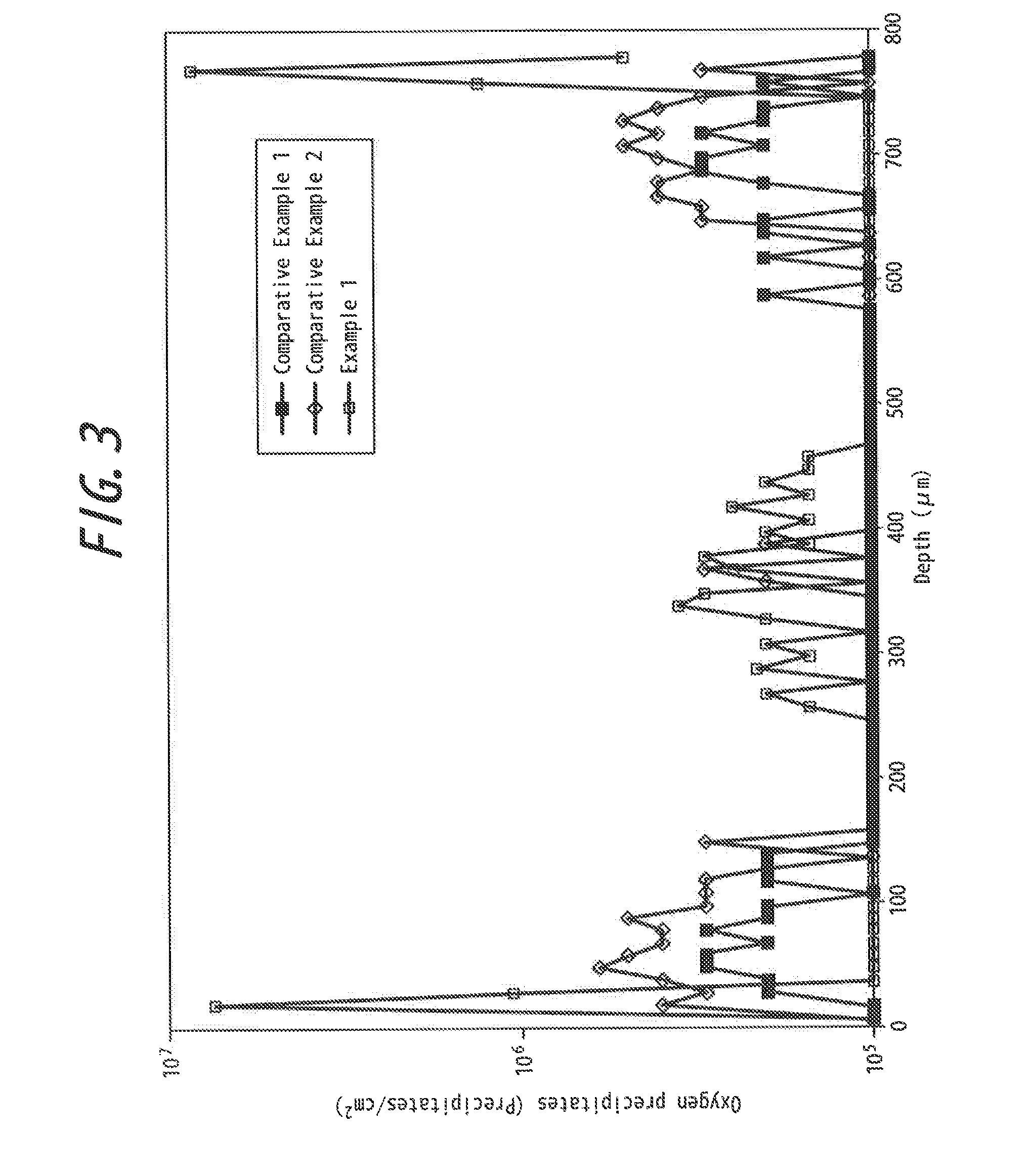
[Solving Means] The present invention is a method of producing an epitaxial substrate, comprising a step of growing an epitaxial layer on a silicon substrate containing carbon as a dopant to form an epitaxial substrate; and, after the formation of the epitaxial substrate, a step of applying a first thermal treatment and a second thermal treatment to the epitaxial substrate such that a density of oxygen precipitates in a surface layer of the silicon substrate constituting the epitaxial substrate is larger than a density of oxygen precipitates at a center of the silicon substrate in a thickness direction.
Description
[0001]The present invention relates to an epitaxial substrate and a method for producing the same, and in particular, relates to an epitaxial substrate for a solid state imaging sensor for use in a digital video camera, cellular phone and the like, and a method for producing the same.RELATED ART[0002]A solid state imaging sensor is produced by: pulling up a silicon single crystal using the Czochralski (CZ) process or the like; slicing the silicon single crystal to obtain a silicon substrate; forming an epitaxial layer on the silicon substrate to obtain an epitaxial substrate; and, forming a circuit on the epitaxial layer. However, when a metal is introduced into the epitaxial substrate as an impurity, the introduced metal causes an increase in dark current of an image sensor, posing a problem of significantly deteriorating electric properties of a solid state imaging sensor such as occurrence of a defect called a white defect.[0003]A factor of the introduction of the metal into the ...
Claims
Login to View More Application Information
Patent Timeline
 IPC IPC(8): C30B33/02B32B5/16
CPCH01L21/3221Y10T428/25H01L21/3225
InventorOMOTE, SHUICHIKURITA, KAZUNARI
OwnerSUMCO CORP