
Method for forming image sensor with shield structures

a shield structure and image sensor technology, applied in the field of image sensors, can solve the problems of reducing the accuracy or image resolution of the image sensor, the solution is not wholly satisfactory, and the imd layer does not improve the photo-efficiency or sensitivity of the image sensor

Active Publication Date: 2012-01-05
SEMICON COMPONENTS IND LLC
View PDF2 Cites 220 Cited by
  • Summary
  • Abstract
  • Description
  • Claims
  • Application Information

AI Technical Summary

Problems solved by technology

This undesirable effect is commonly called cross-talk and results in reduced accuracy or image resolution of the image sensor 100.
This solution is not wholly satisfactory in that depending on the number, location and size of the IMD layers 114A, 114B not all of the light 106A striking at a highly oblique angle will be stopped, and the IMD layers do not improve the photo-efficiency or sensitivity of the image sensor 100.
This requirement in turn causes an increase in the pixel size, or a decrease of the number of pixels within the image sensor.
This approach is also not wholly satisfactory for a number of reasons.
First, as with the other approaches outlined above for light striking the micro-lens array at a highly oblique angle, the lens may be insufficient to redirect all of the light toward the underlying pixel, and away from the adjacent pixel.
Moreover, the fabrication of the micro-lens array and / or mating the array with the pixels of the image sensor can significantly increase the cost and / or decrease the throughput and yield of working devices.

Method used


Image

  • Method for forming image sensor with shield structures
  • Method for forming image sensor with shield structures
  • Method for forming image sensor with shield structures

Examples


Embodiment Construction

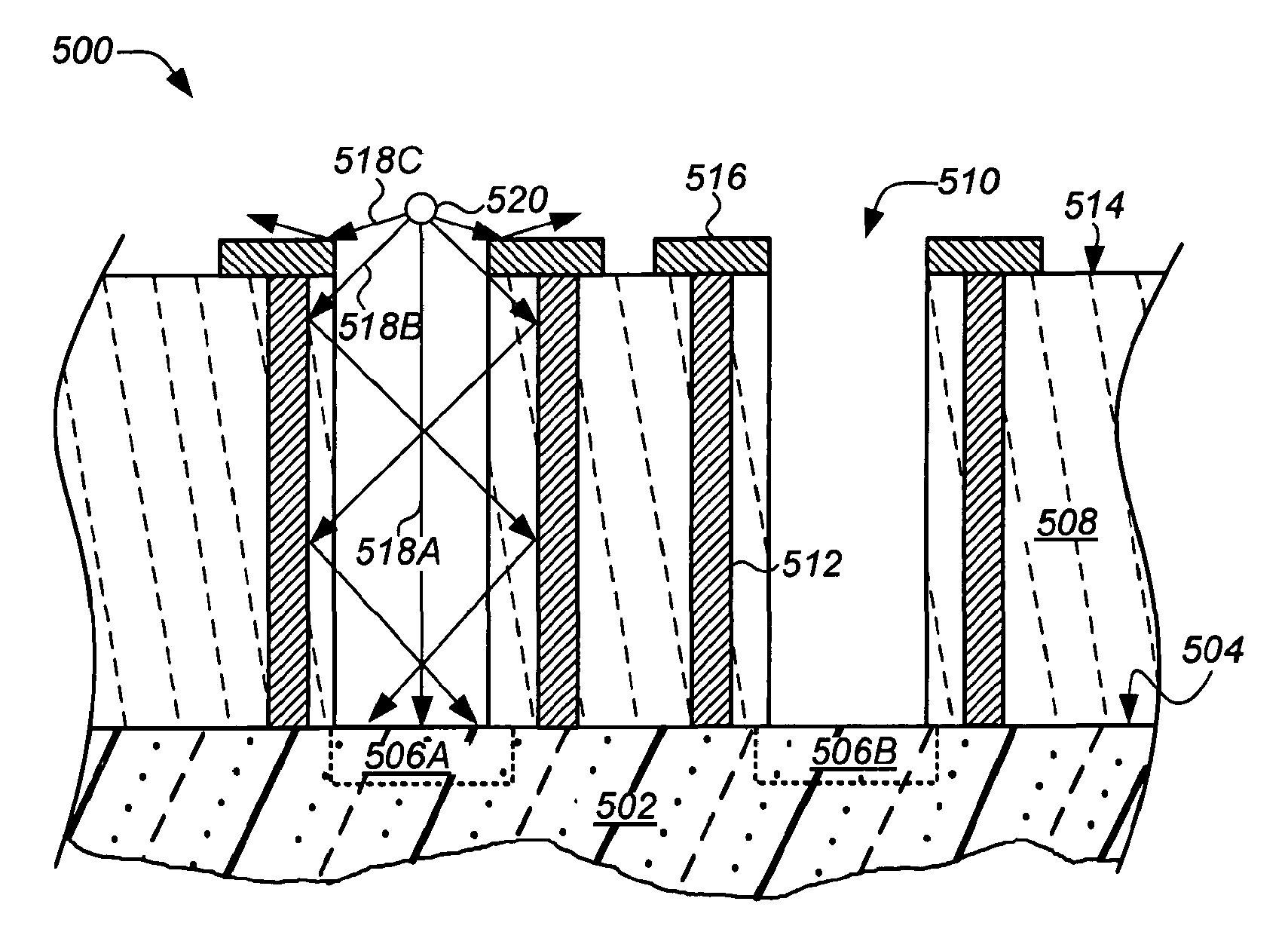
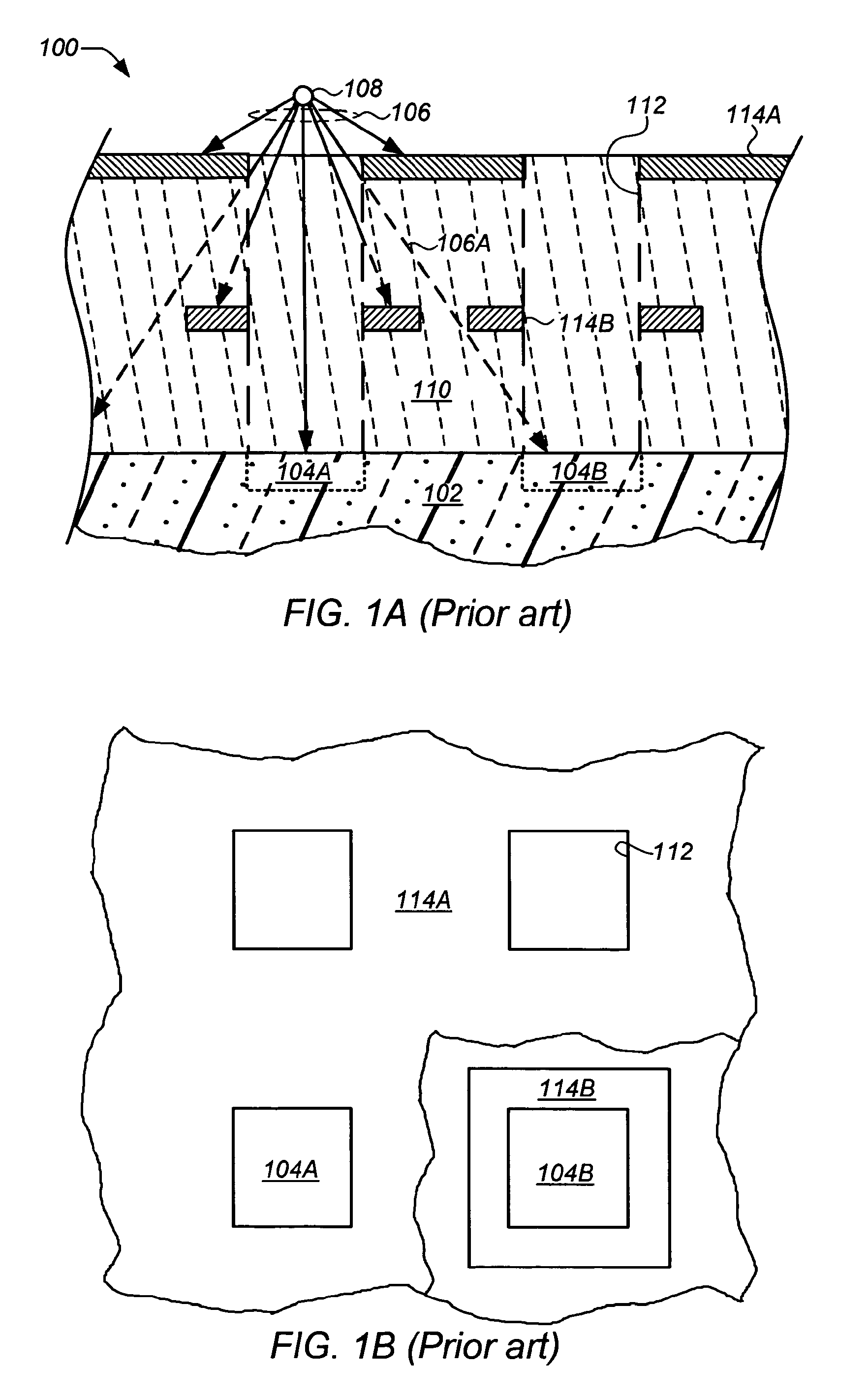
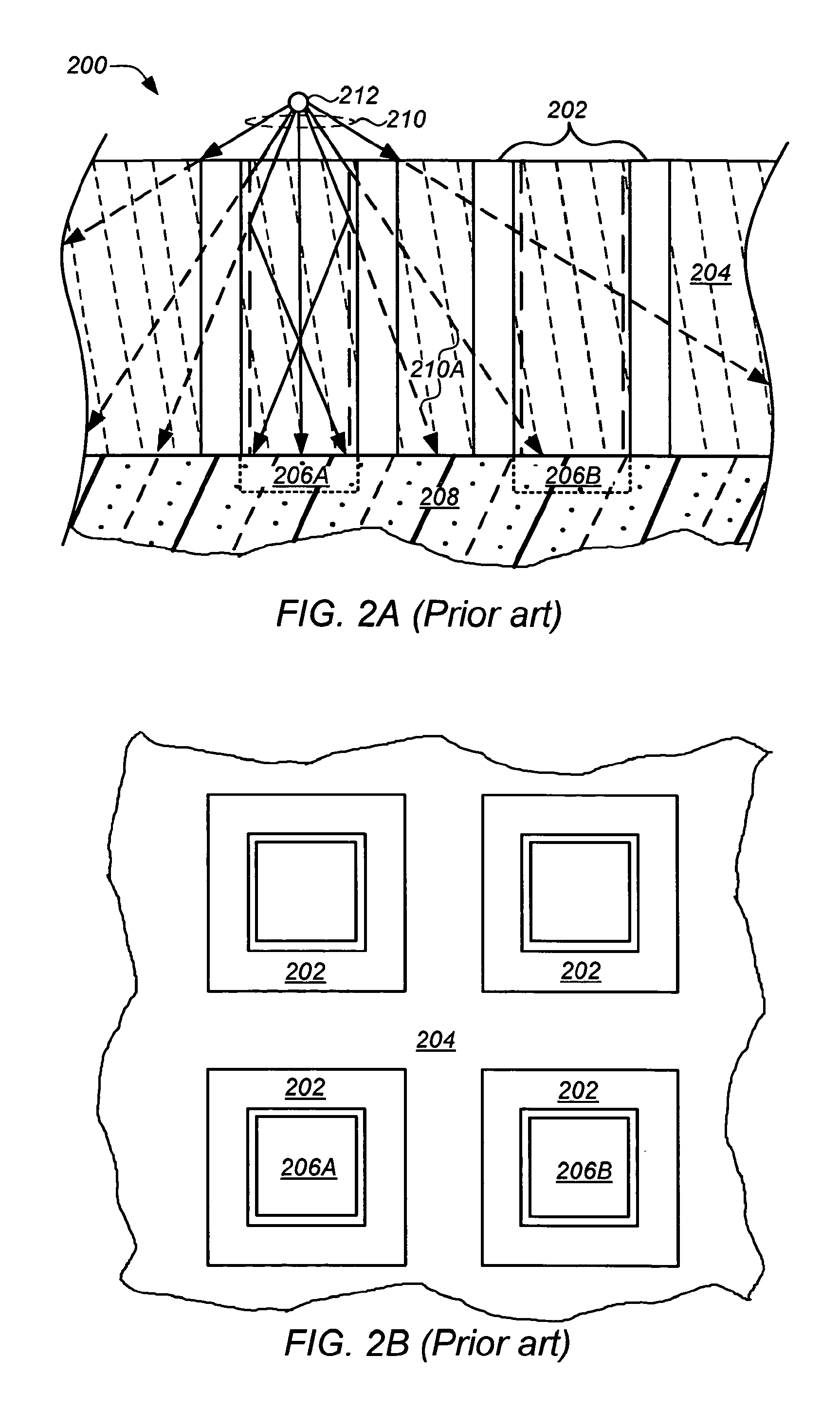
[0019]The present invention is directed to image sensors having an array of multiple photosensitive elements or pixels, and more particularly to image sensors having shield structures to substantially prevent cross-talk between adjacent pixels and to increase photo intensity of light received thereon.

[0020]In the following description, for purposes of explanation, numerous specific details are set forth in order to provide a thorough understanding of the present invention. It will be evident, however, to one skilled in the art that the present invention may be practiced without these specific details. In other instances, well-known structures, and techniques are not shown in detail or are shown in block diagram form in order to avoid unnecessarily obscuring an understanding of this description.

[0021]Reference in the description to “one embodiment” or “an embodiment” means that a particular feature, structure, or characteristic described in connection with the embodiment is included ...


PUM


Abstract

An image sensor having shield structures and methods of forming the same are provided. Generally, the image sensor includes: (i) substrate having at least one photosensitive element formed therein; (ii) a dielectric layer overlying the substrate and the photosensitive element; and (iii) an annular reflective waveguide disposed in the dielectric layer above the photosensitive element to reduce cross-talk between adjacent elements of the sensor while increasing sensitivity of the sensor. In certain embodiments, the sensor further includes a photoshield disposed in the dielectric above the photosensitive element and about the waveguide to further reduce the possibility of cross-talk. Other embodiments are also disclosed.

Description

CROSS-REFERENCE TO RELATED APPLICATIONS[0001]The present application is a divisional application of prior U.S. patent application Ser. No. 11 / 509,480, filed on Aug. 23, 2006, which is hereby incorporated by reference, and priority thereto for common subject matter is hereby claimed.TECHNICAL FIELD[0002]The present invention relates generally to image sensors, and more particularly to image sensors having shield structures to prevent cross-talk between adjacent sensors and to increase photo intensity of light received thereon and methods for forming the same.BACKGROUND OF THE INVENTION[0003]Solid-state image sensors are widely used in a number of optoelectronic applications including digital cameras, cellular phones, and optical navigation or pointing systems, such as optical computer mice, trackballs, touch screens scroll bars and the like. Conventional solid-state image sensors typically include an array of photosensitive elements, such as charge-coupled devices (CCDs) or complemen...

Claims


Application Information

Patent Timeline
Patent Type & Authority Applications(United States)
IPC IPC(8): H01L31/18
CPCH01L27/14625H01L27/14687H01L27/14685
Inventor BYUN, JEONG SOOKOROBOV, VLADIMIRPOHLAND, OLIVER
Owner SEMICON COMPONENTS IND LLC
Features
  • Generate Ideas
  • Intellectual Property
  • Life Sciences
  • Materials
  • Tech Scout
  • Unparalleled Data Quality
  • Higher Quality Content
  • 60% Fewer Hallucinations
Learn More