Electromagnetic interference (EMI) diverter

a technology of electromagnetic interference and diverter, which is applied in the direction of electrical equipment, support structure mounting, rack/frame construction, etc., can solve the problems of unfavorable radio frequency emi environment, undesirable path, and electronic circuit that can withstand more hostile lightening, and achieve low value functional and high dielectric strength

Active Publication Date: 2012-01-12
HONEYWELL INT INC
View PDF5 Cites 4 Cited by
  • Summary
  • Abstract
  • Description
  • Claims
  • Application Information

AI Technical Summary

Benefits of technology

[0023]Surrounding the insulating layer 40 is an exterior casing 50. The exterior casing 50 comprises a conductive enclosure that may be attached to another structure (not shown) via one or more anchor points 51. The exterior casing 50 may be made of any suitable metallic element or alloy. Non-limiting examples of suitable metals include aluminum, iron, nickel, copper, and alloys thereof, such as stainless steel or nickel-chromium based super alloys such as Inconel® made by Special Metals Corporation of New Hartford, N.Y. The exterior casing 50, the inner conductive enclosure 20 / 30 and the insulating layer 40 located therebetween, comprise a low value functional capacitor with a high dielectric strength. The external casing provides protection from the environments and may hermetically seal the external EMI diverter 100. The insulating layer may be secured or potted to the exterior casing 50 with adhesives as needed to achieve mechanical strength and rigidity between the conducting enclosure 20 / 30 and the exterior casing 50.

Problems solved by technology

For example, if a proximity sensor senses that a device or component is within a predetermined distance of a reference location, this may indicate an undesired configuration.
However, the filter capacitors are typically coupled from internal wiring to a chassis and may provide an undesirable path for lightning currents to be conducted into other sensitive electronic equipment connected to the wiring.
Presently, electronic circuits that can withstand more hostile lightening and radio frequency EMI environments are not readily available.

Method used


Image

  • Electromagnetic interference (EMI) diverter
  • Electromagnetic interference (EMI) diverter
  • Electromagnetic interference (EMI) diverter

Examples


Embodiment Construction

[0013]The following detailed description is merely exemplary in nature and is not intended to limit the invention or the application and uses of the invention. As used herein, the word “exemplary” means “serving as an example, instance, or illustration.” Thus, any embodiment described herein as “exemplary” is not necessarily to be construed as preferred or advantageous over other embodiments. All of the embodiments described herein are exemplary embodiments provided to enable persons skilled in the art to make or use the invention and not to limit the scope of the invention which is defined by the claims. Furthermore, there is no intention to be bound by any expressed or implied theory presented in the preceding technical field, background, brief summary, or the following detailed description.

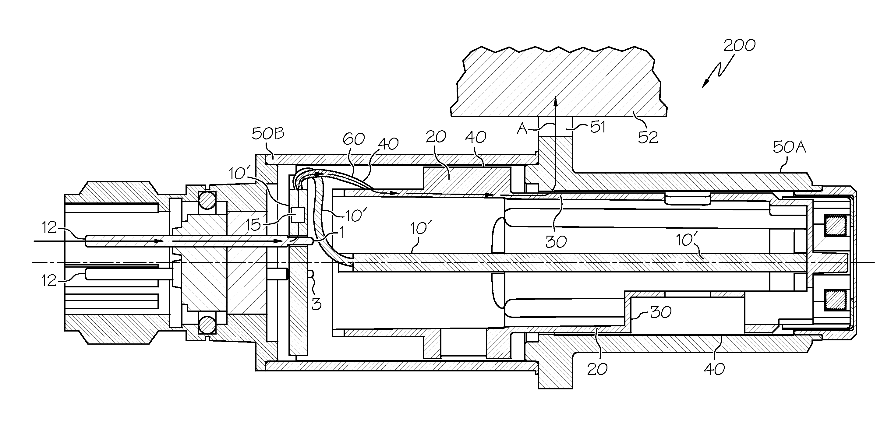
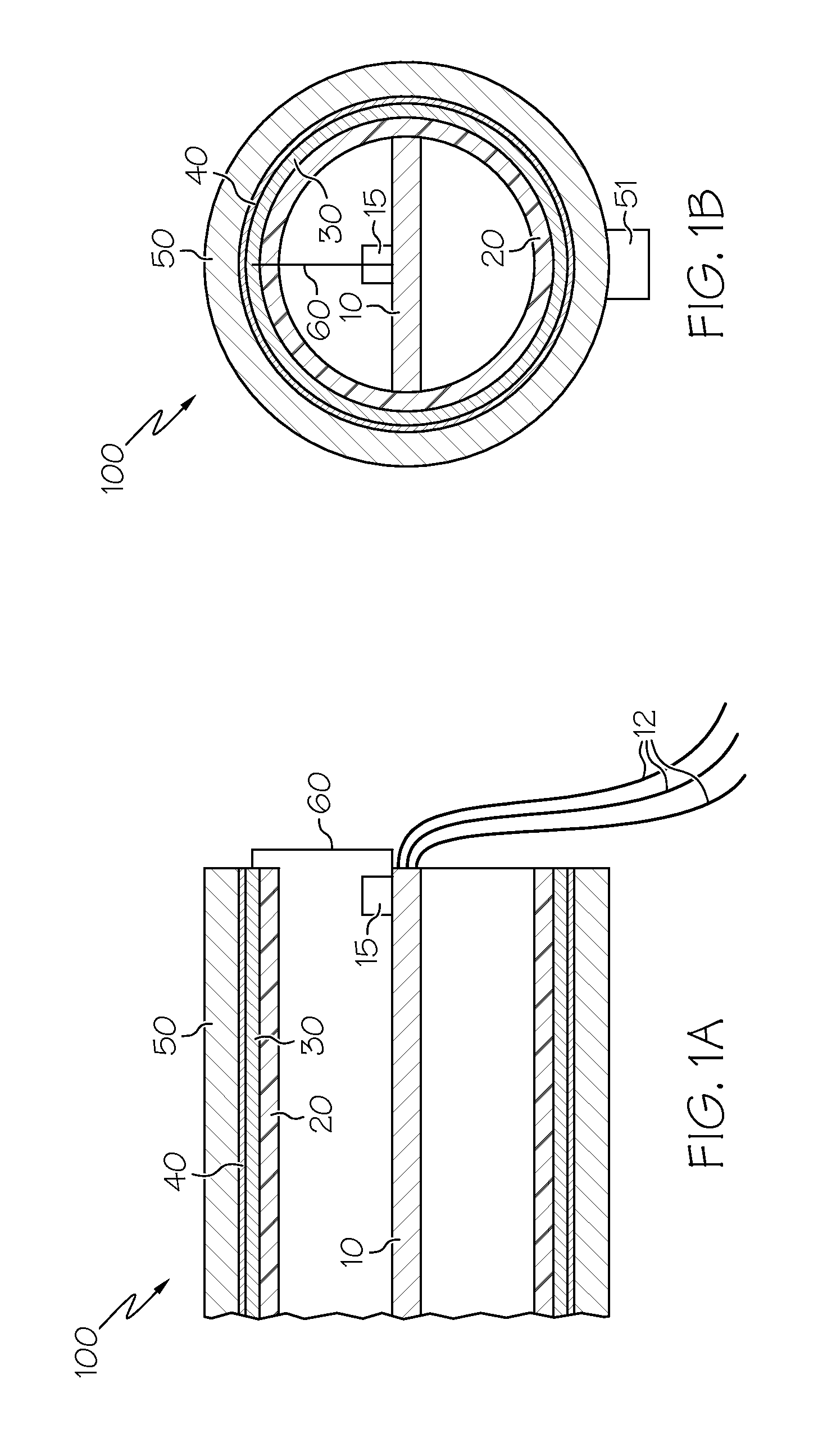
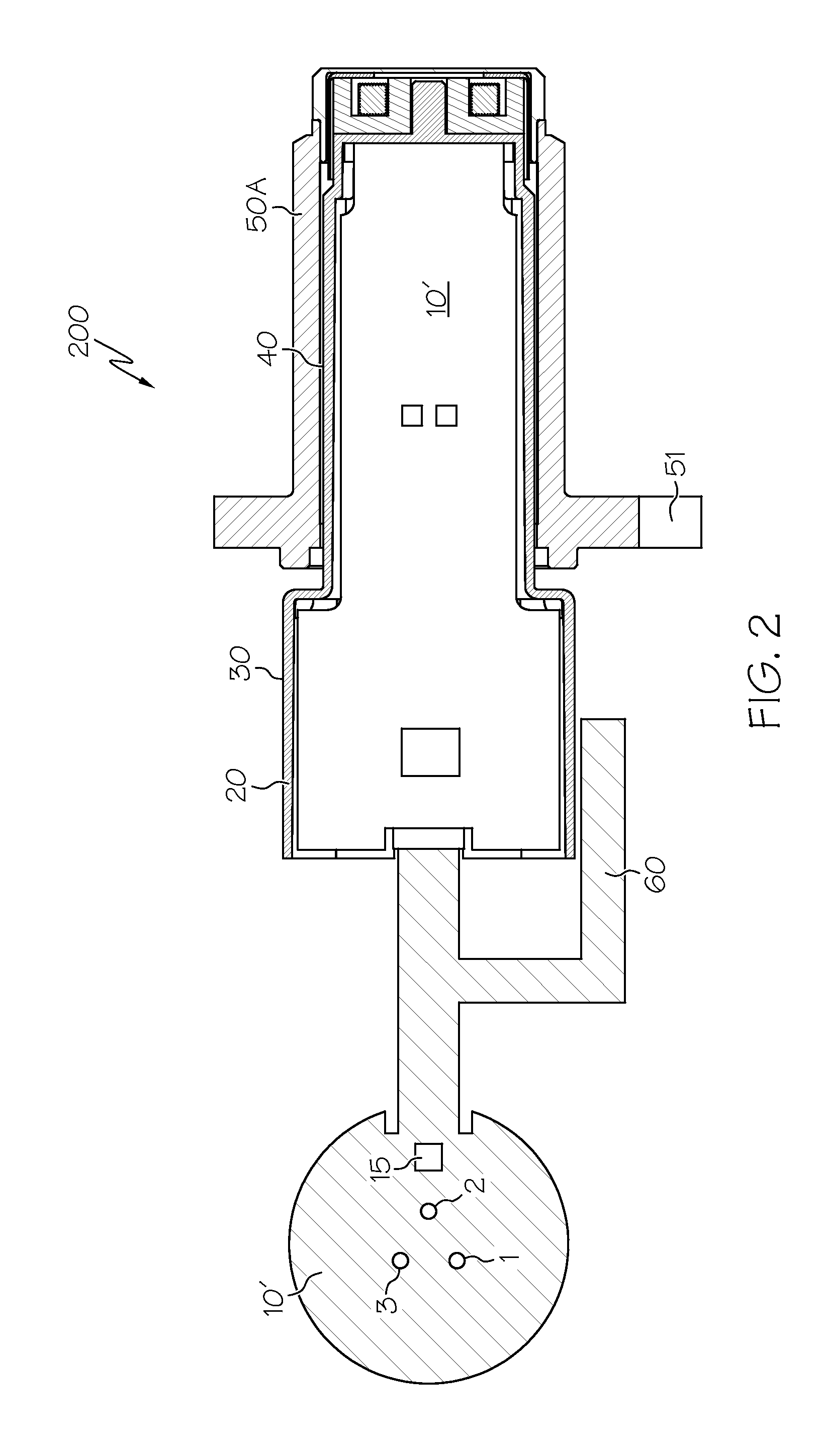
[0014]The exemplary embodiment disclosed herein is an external EMI diverting structure to electrically shield an electronic device or circuit from EMI. The electronic device is isolated from th...


PUM

PropertyMeasurementUnit
electromagnetic interferenceaaaaaaaaaa
metallicaaaaaaaaaa
dielectricaaaaaaaaaa

Abstract

An external EMI diverting structure to electrically shield an electronic device from EMI is presented. The electronic device is physically isolated from the case ground which interrupts the EMI or lightning fault path. This shield provides a return path to ground for the EMI away from the electronic device and replaces conventional EMI filter capacitors, which are not connected to case ground. The external EMI diverter comprises a first conducting enclosure enclosing the electrical circuit and is electrically coupled to the electric circuit and a second conducting enclosure enclosing the first conducting enclosure and being electrically isolated from the first conducting enclosure and the electric circuit. The diverter is physically and electrically connected to the case ground at an attachment point.

Description

TECHNICAL FIELD[0001]The present invention generally relates to electronic circuits, and more particularly relates to circuits that are hardened to lightning and other electromagnetic interference (EMI).BACKGROUND[0002]Proximity sensors and other electronic devices have long been used to sense when a device or component is operating within predefined tolerances. In many instances, the signals generated by a proximity sensor may be used to selectively enable and disable various portions of a system. For example, if a proximity sensor senses that a device or component is within a predetermined distance of a reference location, this may indicate an undesired configuration. In such an instance, the sensor output signal may be used to disable a system (or portion thereof). Conversely, if a device or component being within a predetermined distance of a reference location is a desired configuration, the sensor output signal may be used to enable a system (or a portion thereof).[0003]Sensor...

Claims


Application Information

Patent Timeline
Patent Type & Authority Applications(United States)
IPC IPC(8): H05K9/00H05K13/00
CPCY10T29/49002H05K9/005
Inventor TILLOTSON, JOHN KENNETH
Owner HONEYWELL INT INC
Why Eureka
Try Eureka