Electrostatic discharge protection device for giga-hertz radio frequency integrated circuits with varactor-LC tanks

a radio frequency integrated circuit and varactor technology, applied in the field of radio frequency integrated circuits, can solve the problem that state-of-the-art cmos technology can only make on-chip inductors with low q values, and achieve the effect of low parasitic resistance and high esd level

Inactive Publication Date: 2005-04-26
LIBERTY PATENTS LLC
View PDF6 Cites 61 Cited by
  • Summary
  • Abstract
  • Description
  • Claims
  • Application Information

AI Technical Summary

Benefits of technology

[0012]The capacitance of the varactor is the depletion capacitance of the reverse-biased diode, which can be controlled by adjusting the supplied voltage. The inductor can be implemented as an on-chip device. However, the state-of-the-art CMOS technology can only make on-chip inductor with low Q value. The other choice is to use high Q value inductors, such as a bond-wire inductor. Furthermore, as the values of the inductance and the capacitance of the LC-tank can be designed to resonate at the RF operating frequency, the signal will not be lost to the ground due to the infinite resistance seen by the signal from the input to the ground.
[0013]In an ESD condition, an ESD current flows through the inductor and the varactor of LC tank. The advantage of having multiple paths for the ESD current is to raise the ESD level. Because the inductor is a metal line with low parasitic resistance, the varactor-LC tank has a high ESD level due to the multiple paths for the ESD current.

Problems solved by technology

However, the state-of-the-art CMOS technology can only make on-chip inductor with low Q value.

Method used


Image

  • Electrostatic discharge protection device for giga-hertz radio frequency integrated circuits with varactor-LC tanks
  • Electrostatic discharge protection device for giga-hertz radio frequency integrated circuits with varactor-LC tanks
  • Electrostatic discharge protection device for giga-hertz radio frequency integrated circuits with varactor-LC tanks

Examples


first embodiment

[0027]With reference to the drawings and in particular to FIG. 5, an ESD protection device constructed in accordance with the present invention comprises an ESD circuit arranged in an I / O port of a radio frequency integrated circuit (RFIC), and a secondary circuit comprised of a varactor-LC tank. Since the RFIC application requires a small parasitic capacitance, the ESD device is made small in size while possesses a high ESD level. Examples are an STI diode and an SCR device. In the illustrated embodiment, the varactor comprises a reverse-biased diode. However, other devices of the same electrical characteristics can be employed equally. The capacitance of the varactor is the depletion capacitance of the reverse-biased diode, which can be controlled by adjusting the supplied voltage. The inductor can be implemented as an on-chip device or alternatively, the inductor is embodied by a bond-wire inductor.

[0028]In the embodiment illustrated in FIG. 5, the secondary varactor-LC tank circ...

third embodiment

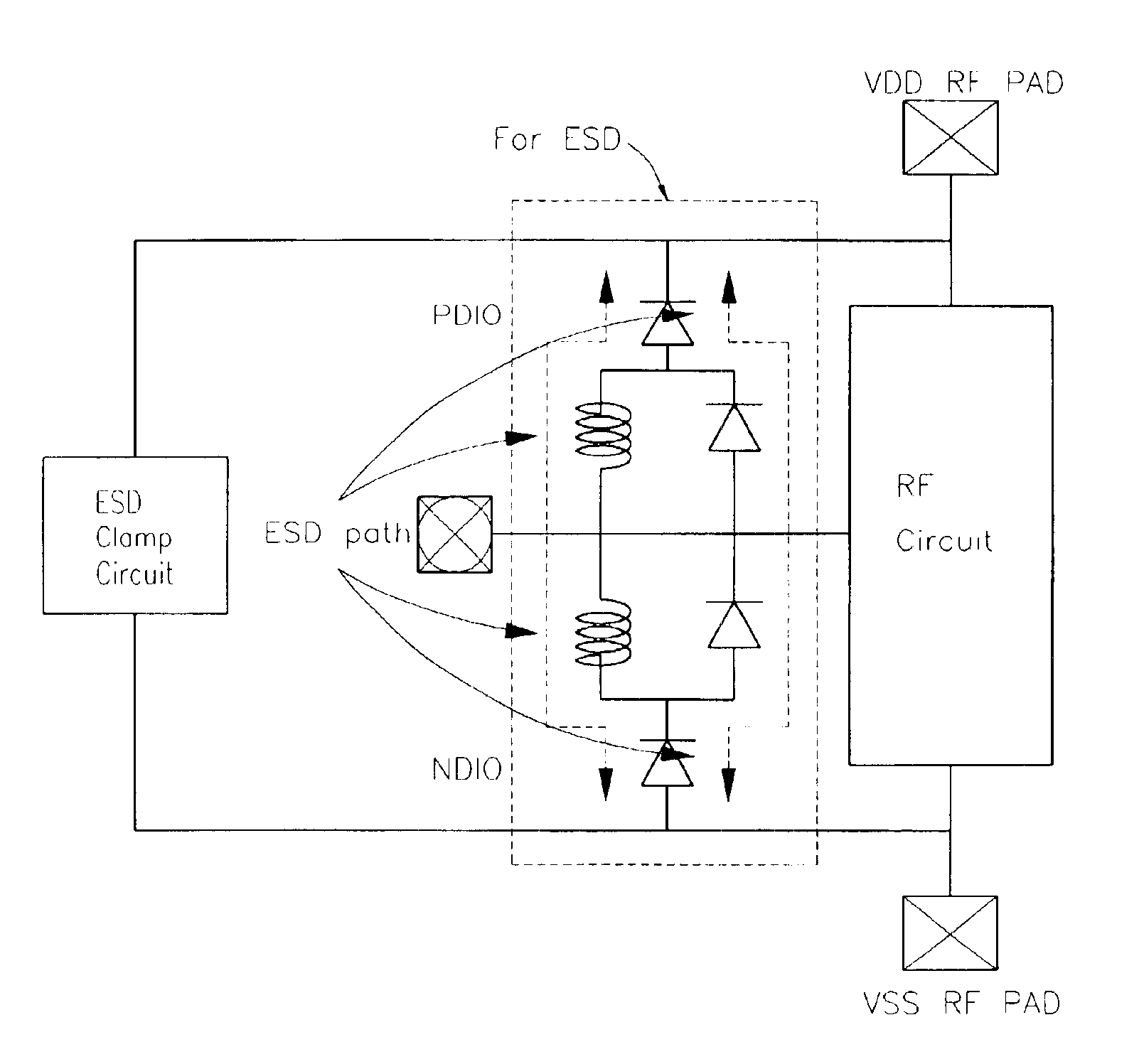
[0032]FIG. 7 shows an ESD protection device in accordance with the present invention in which two varactor-LC tanks are stacked with the diode to achieve higher impedance at resonance. The varactor-LC tank is designed to resonate at the RF operating frequency to avoid power gain loss even when the impedance becomes infinite. The ESD current will flow through inductor L and ESD diode. To avoid the diodes operating in a breakdown condition, and causing a much lower ESD level, a turn-on efficient Vdd-to-Vss clamp circuit between the power rails is built into the ESD protection circuit to significantly increase the ESD level.

[0033]When the RF input pin is zapped in the NS-mode ESD stress, the NDIO diode is operating in the forward-biased condition with inductor to discharge ESD current. The diode operates in a forward-biased condition can sustain a much higher ESD level than in a reverse-biased condition. The Vdd-to-Vss ESD clamp circuit is turned on when the RF-input pad is zapped with...

fifth embodiment

[0036]FIG. 9 shows an ESD protection device in accordance with the present invention in which a multiple of varactor-LC tanks are stacked with a diode.

[0037]FIG. 10 shows a modification of the arrangement shown in FIG. 9 by switching the position of the reverse-biased diode and the stacked varactor-LC tanks. The same protection can be obtained with the modified ESD protection device of FIG. 10.


PUM


Abstract

The present invention relates to a device for protecting high frequency RF integrated circuits from ESD damage. The device comprises at least one varactor-LC circuit tank stacked to avoid the power gain loss by the parasitic capacitance of ESD circuit. The varactor-LC tank could be designed to resonate at the RF operating frequency to avoid the power gain loss from the parasitic capacitance of ESD circuit. Multiple LC-tanks could be stacked for further reduction in the power gain loss. A reverse-biased diode is used as the varactor for both purposes of impedance matching and effective ESD current discharging. Because the inductor is made of metal, both the inductor and the varactor can discharge ESD current when ESD condition happens. It has a high enough ESD level to prevent ESD discharge.

Description

FIELD OF THE INVENTION[0001]This invention relates to the field of radio frequency integrated circuit (RFIC), and more particularly to an electrostatic discharge (ESD) protection for RFIC by employing varactor-LC tanks for ESD discharging.BACKGROUND OF THE INVENTION[0002]Electrostatic discharge (ESD) is a transient process of high-energy transfer from IC outside to inside when IC is floated. The entire discharge process takes about 100 ns for a human-body mode (HBM). In general, hundreds of volts, or even higher, are transferred during an ESD stress. Such a high voltage breaks down the gate oxide of the input stage and causes circuit malfunction. As the thickness of the gate oxide scales down continuously, it is important to provide a protection circuit or device to protect the gate oxide and to discharge ESD stress.[0003]A conventional ESD protection circuit, as shown in FIG. 1 of the attached drawings, is a two-staged protection structure for digital ICs comprising a primary stage...

Claims


Application Information

Patent Timeline
Patent Type & Authority Patents(United States)
IPC IPC(8): H02H9/04H01L27/02
CPCH02H9/046H01L27/0251
Inventor KER, MING-DOULEE, CHENG-MINGLO, WEN-YU
Owner LIBERTY PATENTS LLC
Why Eureka
Try Eureka