Three-dimensional touch sensor
a three-dimensional touch sensor and touch sensor technology, applied in the field of touch sensors, can solve the problems of increasing the volume and manufacturing cost of products, unable to provide wide applications for indirect pressure detection, and complicating users' operation
- Summary
- Abstract
- Description
- Claims
- Application Information
AI Technical Summary
Benefits of technology
Problems solved by technology
Method used
Image

Examples
first embodiment
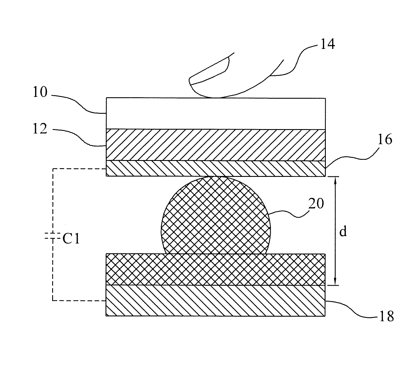
[0021]FIG. 1 is a schematic diagram showing a three-dimensional touch sensor according to the present invention, which includes a protective layer 10, a two-dimensional capacitive touch sensor 12, conductive layers 16 and 18, and an elastic insulator 20. The protective layer 10 is deposited on the two-dimensional capacitive touch sensor 12. As is well known, the two-dimensional capacitive touch sensor 12 has a plurality of sensing electrodes, and when a conductor 14 (e.g. a finger) touches the protective layer 10, the sensing electrodes in the touched area will generate capacitance variations, from which the location of the conductor 14 on the sensing plane can be determined. This disclosure refers the term “sensing plane” to a plane defined by all the sensing electrodes of the two-dimensional capacitive touch sensor 12, for example, in FIG. 1, the top surface of the two-dimensional capacitive touch sensor 12, i.e. the one perpendicular to the paper where the drawing is presented, i...
second embodiment
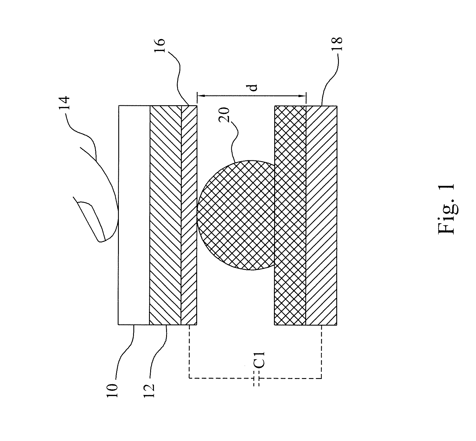
[0022]FIG. 2 is a schematic diagram showing a three-dimensional touch sensor according to the present invention, in which an insulation layer 22 and an elastic conductor 24 are additionally provided below the conductive layer 16, and the insulation layer 22 is sandwiched between the conductive layer 16 and the elastic conductor 24 such that the conductive layer 16 and the elastic conductor 24 are separated by a distance d. Preferably, the elastic conductor 24 has a spherical part contacting the insulation layer 22 in a contact area A, so that the conductive layer 16 and the elastic conductor 24 establish a variable capacitor C2. Pressing the conductor 14 downward leads to the deformation of the elastic conductor 24, and in turn changes the contact area A between the elastic conductor 24 and the insulation layer 22 in size. The greater the pressure is, the larger the contact area A is. According to the equation Eq-1, the variable capacitor C2 has its capacitance varying with the vari...
third embodiment
[0023]FIG. 3 is a schematic diagram showing a third embodiment derived from FIG. 2 by removing the conductive layer 16 and using the sensing electrode of the two-dimensional capacitive touch sensor 12 as an electrode of a variable capacitor C3. Similarly, the insulation layer 22 is sandwiched between and thereby separates the two-dimensional capacitive touch sensor 12 and the elastic conductor 24 by a distance d. The elastic conductor 24 contacts the insulation layer 22 in an area A with its spherical part, so that the elastic conductor 24 and the sensing electrode of the two-dimensional capacitive touch sensor 12 establish the variable capacitor C3. The contact area A varies with the pressure applied by an object 26 in the manner that the greater the pressure is, the larger the contact area A is. According to the equation Eq-1, the variable capacitor C3 has its capacitance varies with the variation of the contact area A, and thus the capacitance variation sensed from the sensing el...
PUM
 Abstract
Description
Claims
Application Information
 - R&D Engineer
- R&D Manager
- IP Professional
- Industry Leading Data Capabilities
- Powerful AI technology
- Patent DNA Extraction
Browse by: Latest US Patents, China's latest patents, Technical Efficacy Thesaurus, Application Domain, Technology Topic.
© 2024 PatSnap. All rights reserved.Legal|Privacy policy|Modern Slavery Act Transparency Statement|Sitemap