
Microelectronic elements having metallic pads overlying vias

Active Publication Date: 2012-01-26
TESSERA INC
View PDF6 Cites 186 Cited by
  • Summary
  • Abstract
  • Description
  • Claims
  • Application Information

AI Technical Summary

Benefits of technology

[0034]Further aspects of the invention provide systems which incorporate microelectronic structures according to the foregoing aspects of the invention, composite chips according to the foregoing aspects of the invention, or both in conjunction with other electronic devices. For example, the system may be disposed in a single housing, which may be a portable housing. Systems according to preferred embodiments in this aspect of the invention may be more compact than comparable conventional systems.

Problems solved by technology

Such a reduction in the available space on the first face that can be used for active circuitry may increase the amount of silicon required to produce each semiconductor chip, thereby potentially increasing the cost of each chip.
Conventional vias may have reliability challenges because of a non-optimal stress distribution inside of the vias and a mismatch of the coefficient of thermal expansion (CTE) between a semiconductor chip, for example, and the structure to which the chip is bonded.
For example, when conductive vias within a semiconductor chip are insulated by a relatively thin and stiff dielectric material, significant stresses may be present within the vias.
In addition, when the semiconductor chip is bonded to conductive elements of a polymeric substrate, the electrical connections between the chip and the higher CTE structure of the substrate will be under stress due to CTE mismatch.

Method used


Image

  • Microelectronic elements having metallic pads overlying vias
  • Microelectronic elements having metallic pads overlying vias
  • Microelectronic elements having metallic pads overlying vias

Examples


Embodiment Construction

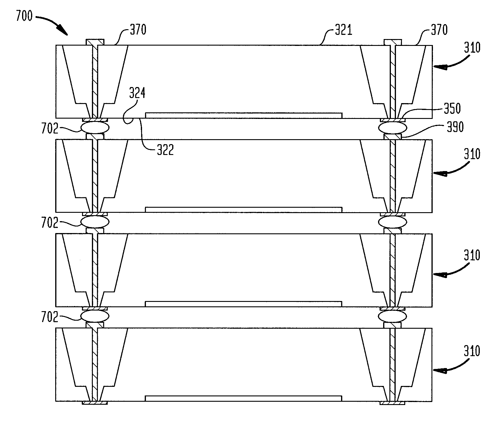
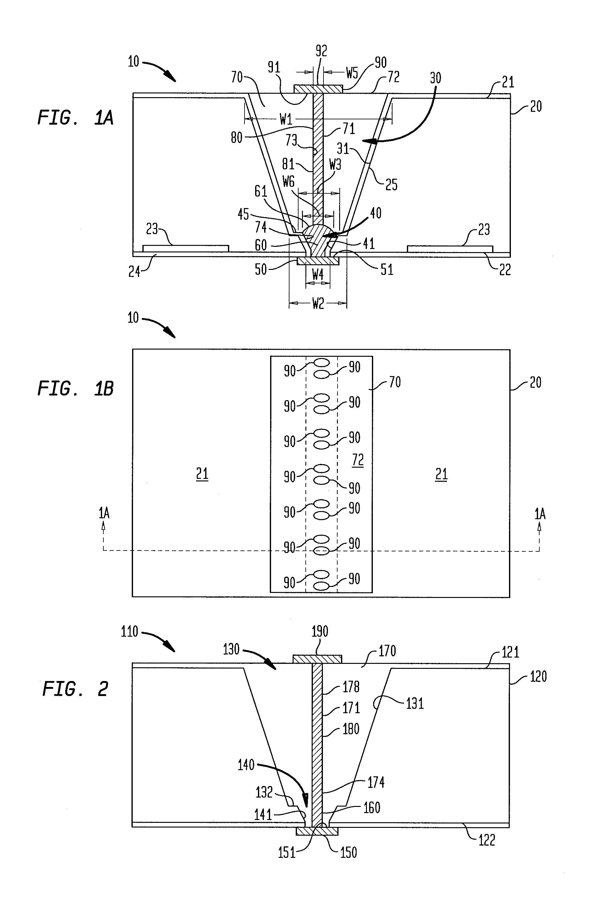
[0069]FIGS. 1A and 1B are a sectional view and a corresponding top-down plan view illustrating a via structure in accordance with an embodiment of the invention. As illustrated in FIGS. 1A and 1B, a microelectronic unit 10 includes a semiconductor element 20 having a first opening 30 extending from a rear surface 21 partially through the semiconductor element 20 towards a front surface 22 and a second opening 40 extending from the first opening 30 to a bottom surface of a conductive pad 50, a conductive via 60 extending within the second opening 40, a dielectric region 70 overlying an inner surface 31 in the first opening 30, a conductive interconnect 80 extending within the first opening 30, and a conductive contact 90 electrically connected to the conductive interconnect 80. The conductive contact 90 can overlie an inner surface 31 of the first opening and may wholly overlie the inner surface 31 or a lower surface 45 or both.

[0070]The semiconductor element 20 can include a semicon...


PUM


Abstract

A microelectronic unit, an interconnection substrate, and a method of fabricating a microelectronic unit are disclosed. A microelectronic unit can include a semiconductor element having a plurality of active semiconductor devices therein, the semiconductor element having a first opening extending from a rear surface partially through the semiconductor element towards a front surface and at least one second opening, and a dielectric region overlying a surface of the semiconductor element in the first opening. The microelectronic unit can include at least one conductive interconnect electrically connected to a respective conductive via and extending away therefrom within the aperture. In a particular embodiment, at least one conductive interconnect can extend within the first opening and at least one second opening, the conductive interconnect being electrically connected with a conductive pad having a top surface exposed at the front surface of the semiconductor element.

Description

BACKGROUND OF THE INVENTION[0001]The present invention relates to packaging of microelectronic devices, especially the packaging of semiconductor devices.[0002]Microelectronic elements generally comprise a thin slab of a semiconductor material, such as silicon or gallium arsenide, commonly called a die or a semiconductor chip. Semiconductor chips are commonly provided as individual, prepackaged units. In some unit designs, the semiconductor chip is mounted to a substrate or chip carrier, which is in turn mounted on a circuit panel, such as a printed circuit board.[0003]The active circuitry is fabricated in a first face of the semiconductor chip (e.g., a front surface). To facilitate electrical connection to the active circuitry, the chip is provided with bond pads on the same face. The bond pads are typically placed in a regular array either around the edges of the die or, for many memory devices, in the die center. The bond pads are generally made of a conductive metal, such as cop...

Claims


Application Information

Patent Timeline
IPC IPC(8): H01L25/10H01L23/528H01L21/768H01L27/07
CPCH01L23/3114H01L2224/133H01L25/0657H01L2225/06513H01L2225/06541H01L2225/06565H01L2924/01029H01L2924/01322H01L2924/0002H01L2924/00014H01L24/03H01L24/05H01L24/06H01L24/13H01L24/16H01L2224/0557H01L2224/05571H01L2224/06181H01L2224/13009H01L2224/13025H01L2224/13111H01L2224/13147H01L2224/16146H01L2224/94H01L23/481H01L2224/131H01L2224/1329H01L2224/0401H01L2924/07811H01L2924/1461H01L2924/12041H01L2924/00012H01L2224/03H01L2924/00H01L2924/014H01L2224/05552H01L27/14618H01L27/14634H01L27/14636H01L2924/14H01L23/48
Inventor OGANESIAN, VAGEMOHAMMED, ILYASMITCHELL, CRAIGHABA, BELGACEMSAVALIA, PIYUSH
Owner TESSERA INC
Features
  • Generate Ideas
  • Intellectual Property
  • Life Sciences
  • Materials
  • Tech Scout
  • Unparalleled Data Quality
  • Higher Quality Content
  • 60% Fewer Hallucinations
Learn More