Socket and method of fabricating the same
- Summary
- Abstract
- Description
- Claims
- Application Information
AI Technical Summary
Benefits of technology
Problems solved by technology
Method used
Image

Examples
first embodiment
Socket Structure in First Embodiment
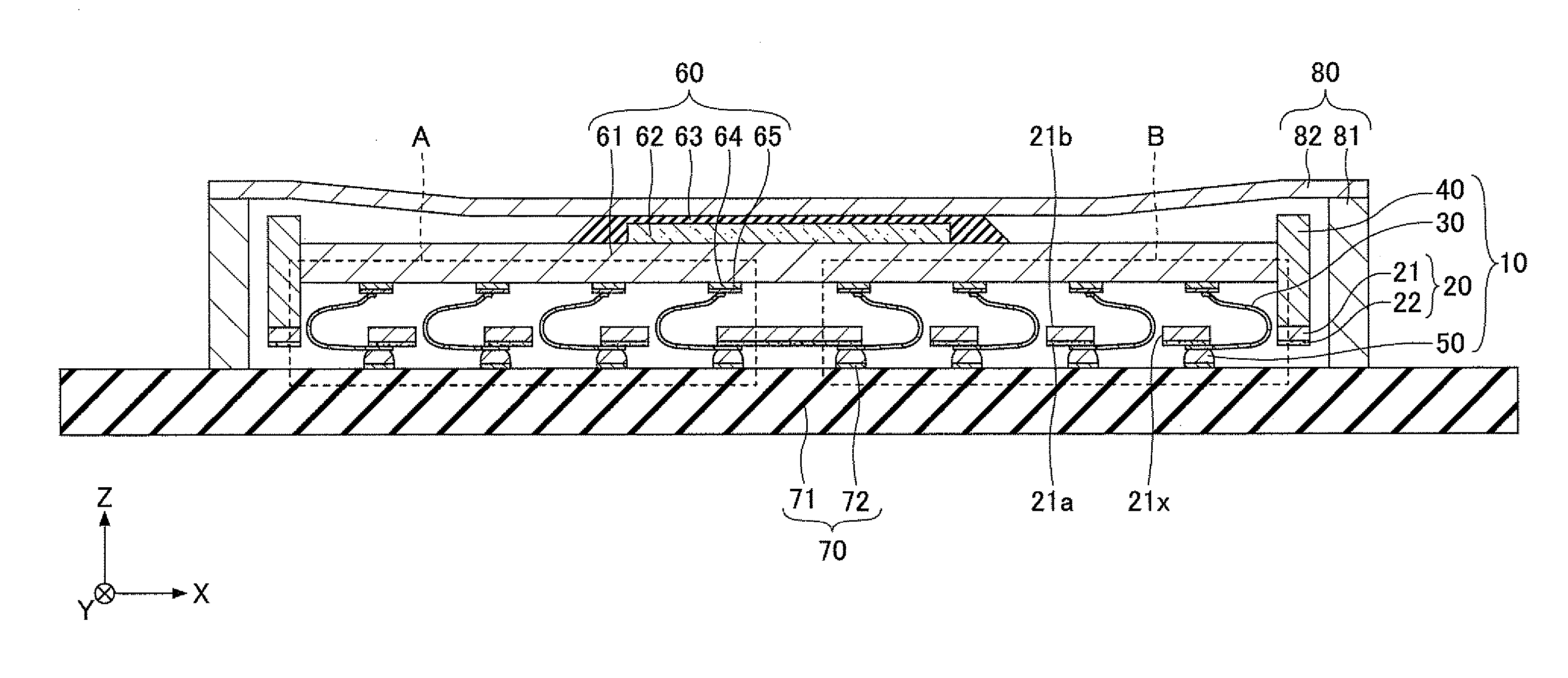
[0054]FIG. 4 is a cross sectional view illustrating a socket in a first embodiment of the present invention, and FIG. 5 is a cross sectional view illustrating a part of the socket illustrated in FIG. 4 on an enlarged scale. As illustrated in FIGS. 4 and 5, a socket 10 includes a support member 20, connecting terminals 30, a positioning part 40, and bumps 50. As will be described later, the positioning parts 40 and the bumps 50 may not necessarily be essential elements of the socket 10 that includes the support member 20 and the connecting terminals 30.
[0055]A semiconductor package 60 is an example of a connecting item. The semiconductor package 60 is provided on a circuit board 70, such as a mother board, and covered by a housing 80. The semiconductor package 60 is electrically connected to the circuit board 70 via the socket 10. In this first embodiment, the semiconductor package 60 is used as an example of the connecting item, however, the conn...
first modification
of First Embodiment
[0121]In the first embodiment, the connecting terminals 30 are oriented in parallel with respect to the direction in which the connecting terminals 30 are arranged, as illustrated in FIG. 14. But in a first modification of the first embodiment, the connecting terminals 30 are oriented in a direction that is inclined (or oblique) with respect to the direction in which the connecting terminals 30 are arranged. A description of those parts of the first modification that are the same as those corresponding parts of the first embodiment will be omitted.
[0122]FIG. 18 is a diagram illustrating an example of an arrangement of the connecting terminals in this first modification of the first embodiment. As illustrated in FIG. 18, the connecting terminals 30 are oriented at a predetermined angle θ2 (>0) with respect to a direction E in which the connecting terminals 30 are arranged. In other words, the orientation of the connecting terminals 30 is inclined with respect to th...
second modification
of First Embodiment
[0125]In the first embodiment, one end of the connecting terminal 30 (the surface 31b of the first connecting part 31) is bonded to and electrically connected to the conductor layer 72 of the circuit board 70 via the bump 50. But in a second modification of the first embodiment, a bump 50A may make contact with and be separable from the conductor layer 72 of the circuit board 70. One end of the connecting terminal 30 (surface 31b of the first connecting part 31) makes contact with and electrically connects to the conductor layer 72 of the circuit board 70 via the bump 50A, in a state in which the bump 50A may separate from (that is, not fixed to) the bonding layer 72.
[0126]FIG. 19 is a cross sectional view illustrating an example of a socket in this second modification of the first embodiment. FIG. 20 is a cross sectional view illustrating a part of the socket illustrated in FIG. 19 on an enlarged scale. FIG. 21A is a cross sectional view illustrating connecting t...
PUM
 Abstract
Description
Claims
Application Information
 - R&D
- Intellectual Property
- Life Sciences
- Materials
- Tech Scout
- Unparalleled Data Quality
- Higher Quality Content
- 60% Fewer Hallucinations
Browse by: Latest US Patents, China's latest patents, Technical Efficacy Thesaurus, Application Domain, Technology Topic, Popular Technical Reports.
© 2025 PatSnap. All rights reserved.Legal|Privacy policy|Modern Slavery Act Transparency Statement|Sitemap|About US| Contact US: help@patsnap.com