

Cross-Talk Suppression in Geiger-Mode Avalanche Photodiodes
a technology of avalanche photodiodes and cross-talk suppression, which is applied in the field of electromechanical photodiodes, can solve the problems of optical cross-talk becoming an increasingly limiting source of secondary photon detection, affecting the detection efficiency of secondary photons, and causing current rises. to achieve the effect of suppressing cross-talk effects
- Summary
- Abstract
- Description
- Claims
- Application Information
AI Technical Summary
Benefits of technology
Problems solved by technology
Method used
Image

Examples
example 1
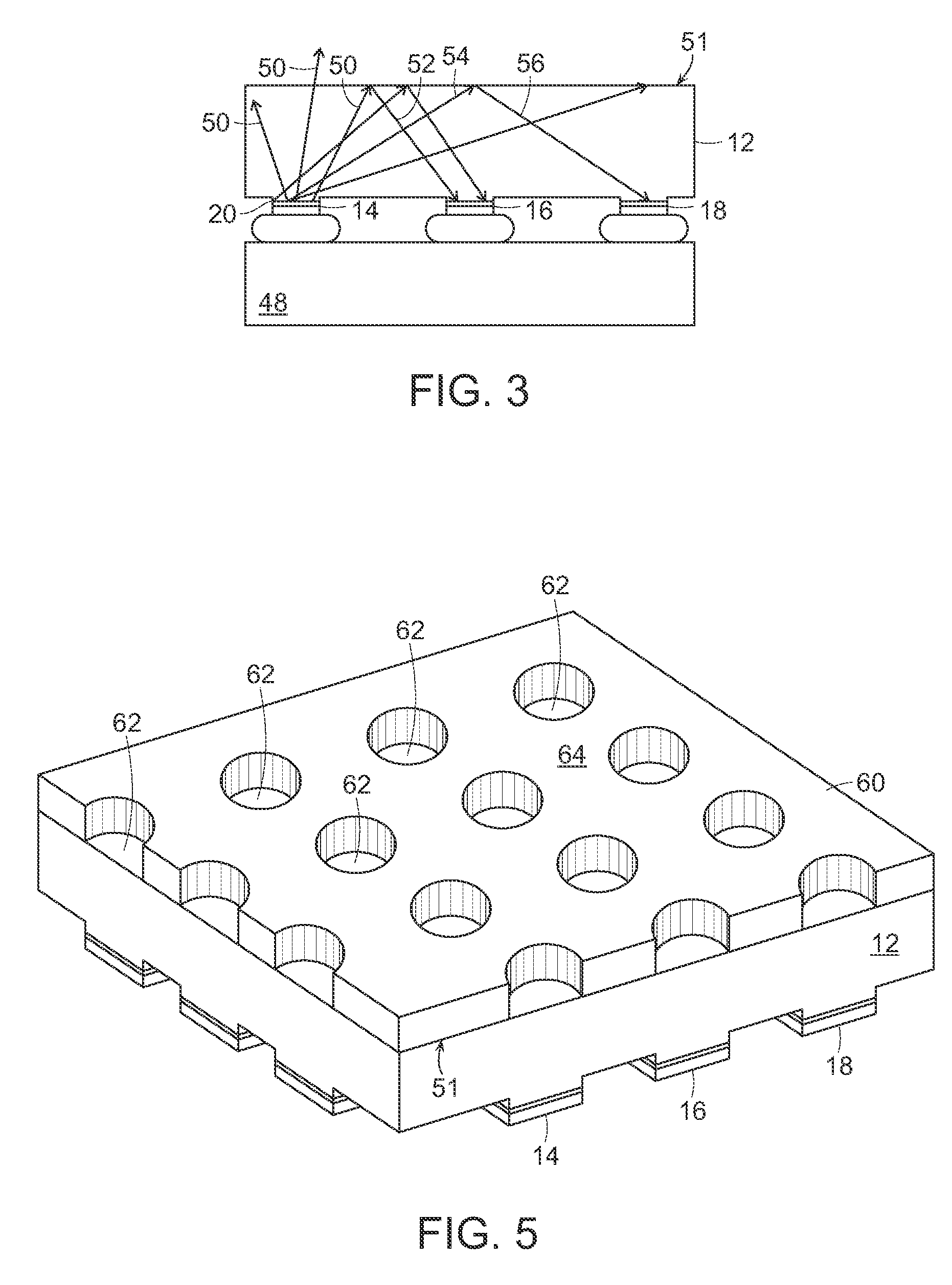
[0048]An APD array substrate of InP was fabricated with mesa photodiodes of the SAM configuration and with no back side surface cross-talk blocking layer. A second InP APD array was similarly produced but was provided with a back-surface cross-talk blocking layer having 40 micron-diameter circular openings, each opening located above an underlying photodiode mesa, with a resulting 50 micron-pitch. The back surface cross-talk blocking layer consisted of a blanket coating of titanium of 50 nm in thickness and a blanket coating of gold of 250 nm in thickness, with the circular openings produced by lift-off photolithography on the titanium and gold layers.
[0049]The optical cross-talk between neighboring photodiodes in a 9×9 area was determined for each of the APD arrays as a function of applied over bias to each photodiode for arming the photodiodes above breakdown to detect incoming photons. FIG. 7 is a plot of an integrated cross-talk probability corresponding to this determination. S...
example 2
[0085]An APD array including photodiodes having the configuration illustrated in FIG. 12 was fabricated with the semiconductor alloy layers specified in FIG. 12. The thicknesses and compositions of the layers were as follows: 1.5 μm-thick In. 89 Ga.11 As.23 P.77 absorber layer, having a 1055 nm bandgap, 1.4 μm-thick InP multiplier layer, 1 μm-thick In.92 Ga.08 As.16 P.84 spectral filter layer, having a 1011 nm bandgap. A similar APD array was fabricated, but not including the spectral filter layer. The thicknesses and compositions of the layers were as follows: 1.5 μm-thick In.81 Ga.19 As.42 P.58 absorber layer, having a 1175 nm bandgap, and a 1.4 μm-thick InP multiplier layer. Both APD arrays included a back-side cross-talk blocking layer. For the array including a spectral filter layer a 50 nm-thick Ge layer and a 25 nm-thick Cr layer were deposited on the back surface. For the APD array without a spectral filter layer the back surface layer consisted of a coating of titanium of 5...
PUM
 Abstract
Description
Claims
Application Information