
Compact sensor package structure

Inactive Publication Date: 2012-02-02
SIGURD MICROELECTRONICS CORP
View PDF6 Cites 21 Cited by
  • Summary
  • Abstract
  • Description
  • Claims
  • Application Information

AI Technical Summary

Benefits of technology

[0007]The primary objective of the present invention is to provide a compact sensor package structure, which has two independent rooms respectively accommodating an LED chip and a sensor chip, and which not only has a smaller volume but also prevents the sensor chip from being interfered with by the light emitted by the LED chip, whereby the present invention has improved performance.

Problems solved by technology

Therefore, the conventional distance sensor has complicated assembly procedures, longer fabrication processes and higher fabrication cost.
Besides, the conventional distance sensor has merely a single sensor chip and thus can only detect limited distance.

Method used


Image

  • Compact sensor package structure
  • Compact sensor package structure
  • Compact sensor package structure

Examples


first embodiment

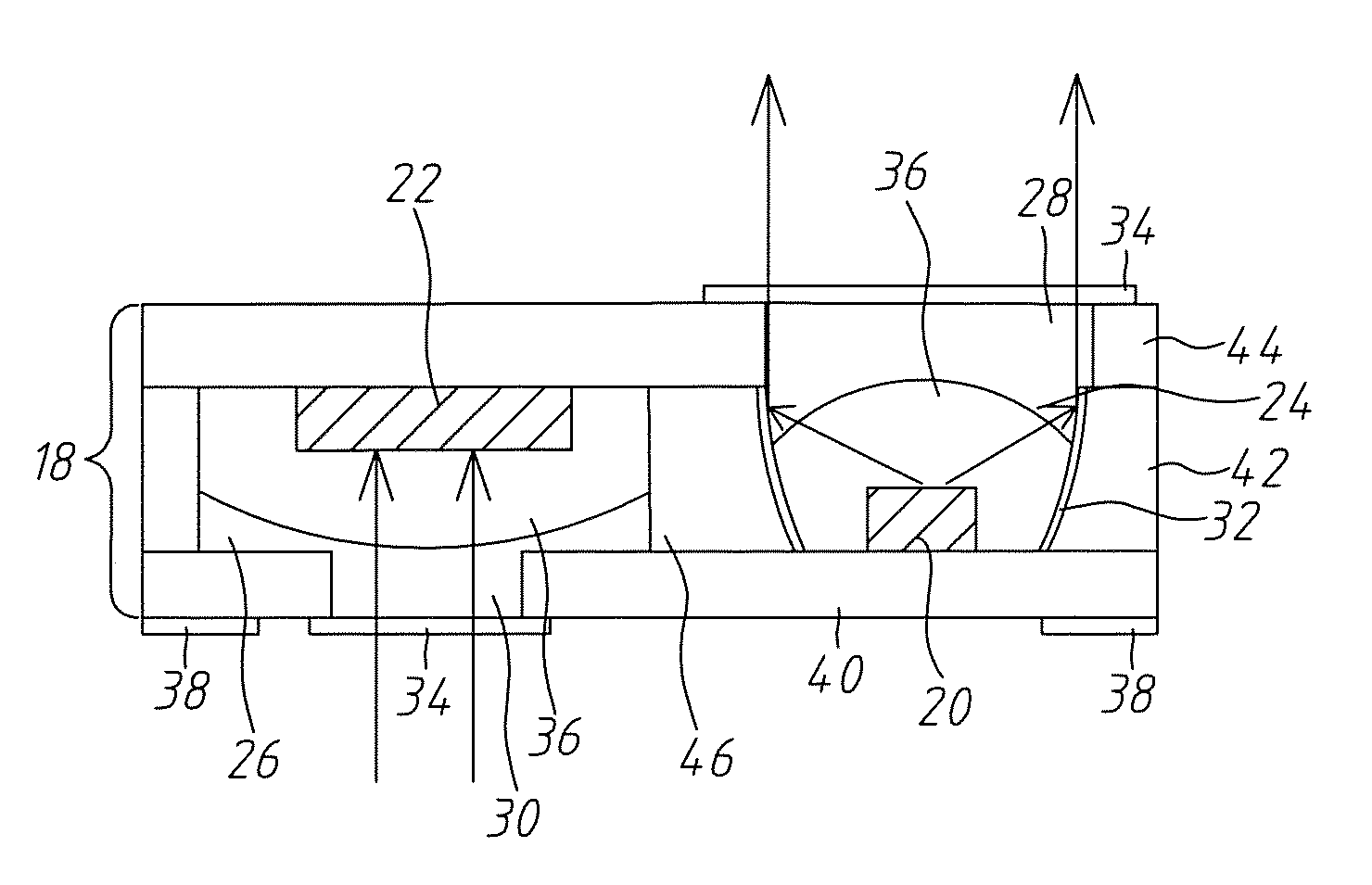
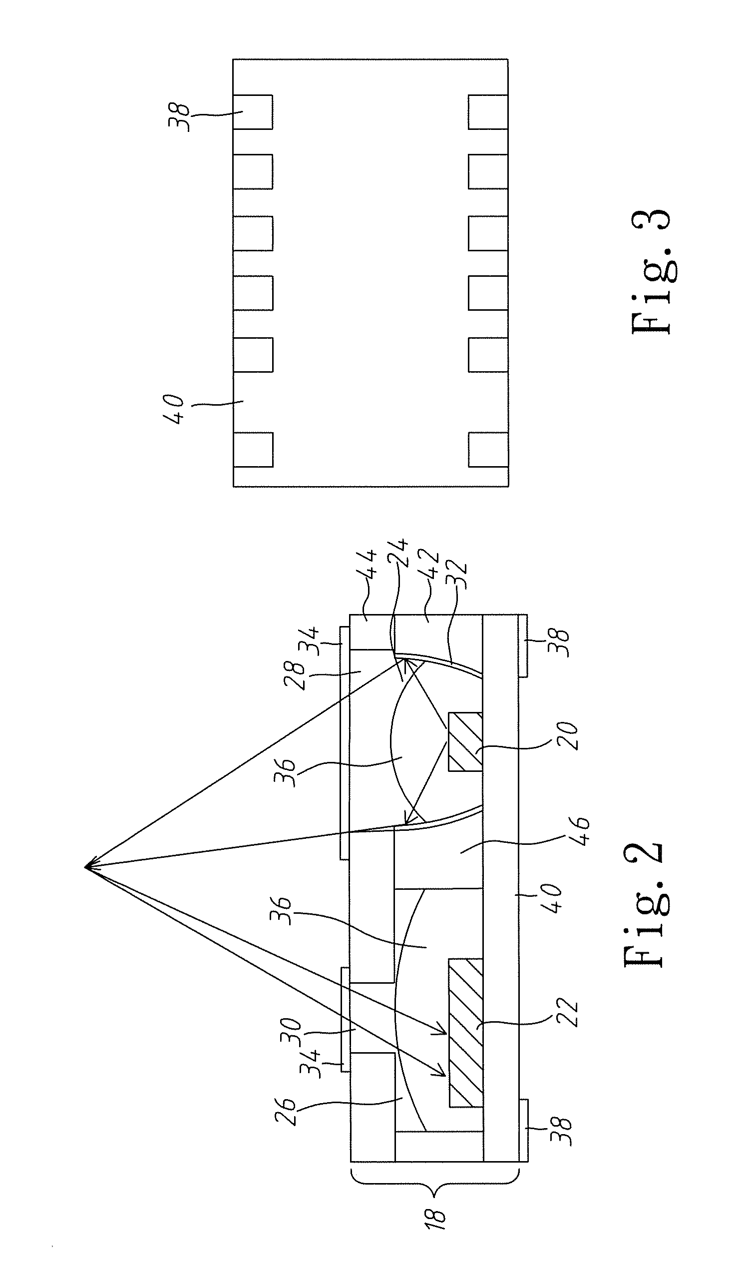
[0015]Below is described a first embodiment according to the present invention. Refer to FIG. 2 and FIG. 3. The compact sensor package structure of the present invention comprises a package body 18, an LED chip 20 and a sensor chip 22. The package body 18 has a first room 24 and a second room 26, which are independent to each other. The package body 18 also has a first hole 28 and a second hole 30. The first hole 28 interconnects the interior and the external environment of the first room 24. The second hole 30 interconnects the interior and the external environment of the second room 26. The second hole 30 is an opening for receiving and focusing light. The second hole 30 is only for receiving a light having a specified range of wavelengths and coming from a specified range of reflective angles lest noise interfere with the sensor chip 22. The inner surface of the first room 24 has a very smooth focusing reflection layer 32. The LED chip 20 is arranged inside the first room 24, cor...

second embodiment

[0021]In the second embodiment, the compact sensor package structure of the present invention comprises a package body 18, an LED chip 20 and a sensor chip 22. The package body 18 has a first room 24 and a second room 26, which are independent to each other. The package body 18 also has a first hole 28 and a second hole 30. The first hole 28 interconnects the interior and the external environment of the first room 24. The second hole 30 interconnects the interior and the external environment of the second room 26. The second hole 30 is only for receiving a light having a specified range of wavelengths and coming from a specified range of reflective angles lest noise interfere with the sensor chip 22. The inner surface of the first room 24 has a very smooth focusing reflection layer 32. The LED chip 20 is arranged inside the first room 24, corresponding to the first hole 28 and below the first hole 28. The focusing reflection layer 32 focuses the light emitted by the LED chip 20 into...


PUM


Abstract

The present invention discloses a compact sensor package structure, which comprises a package body, an LED chip and a sensor chip. The package body has a first room, a second room, a first hole and a second hole. The first and second rooms are independent to each other. The first and second holes interconnect the interiors and the external environments of the first and second rooms. The LED chip is arranged inside the first room, corresponding to the first hole and below the first hole. The LED chip projects light through the first hole. The sensor chip is arranged inside the second room, corresponding to the second hole and above / below the second hole. The sensor chip receives light via the second hole. The present invention features two independent rooms for two chips and prevents interference between the two chips.

Description

BACKGROUND OF THE INVENTION[0001]1. Field of the Invention[0002]The present invention relates to a package structure, particularly to a compact sensor package structure.[0003]2. Description of the Related Art[0004]Sensors and controllers are basic electronics. In sensation, a sensor normally sends a signal, which is normally in form of light, to a detected object; then the signal, which has carried information, is reflected from the detected object back to the sensor for succeeding processing. Refer to FIG. 1. Considering difference between the physical characteristics of the elements and optimization the performance thereof, a light source chip 10 and a sensor chip 12 are normally fabricated and packaged respectively and then electrically connected by a printed circuit board 14, whereby they can detect an object 16.[0005]For example, a conventional distance sensor has two chips. One is an LED (Light Emitting Diode) chip, and the other one is a light sensor chip. The two chips are f...

Claims


Application Information

Patent Timeline
IPC IPC(8): H01L31/12
CPCH01L27/14618H01L25/167H01L2924/0002H01L2924/00
Inventor YEH, TSAN-LIENWU, WAN-HUAPANG, SZU-CHUANWU, CHI-CHANGHUNG, MING-HUNG
Owner SIGURD MICROELECTRONICS CORP
Features
  • Generate Ideas
  • Intellectual Property
  • Life Sciences
  • Materials
  • Tech Scout
  • Unparalleled Data Quality
  • Higher Quality Content
  • 60% Fewer Hallucinations
Learn More