

Solid-state imaging device, method for driving solid-state imaging device, and electronic apparatus
- Summary
- Abstract
- Description
- Claims
- Application Information
AI Technical Summary
Benefits of technology
Problems solved by technology
Method used
Image

Examples
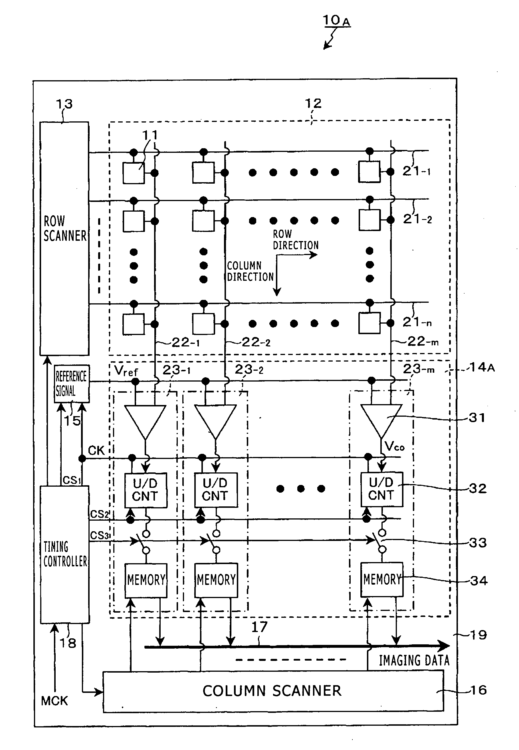
first embodiment
Operation and Effects of First Embodiment
[0120]In the CMOS image sensor 10A equipped with column-parallel ADCs, the following operation and effects can be achieved by reading out the reset level of a unit pixel from which readout of the signal level has been already completed and setting the reset level as the reference voltage of the AD conversion circuit 23 before readout of the signal level of a certain unit pixel. Specifically, difference due to large characteristic fluctuation in the plane (in-plane distribution) and an offset component dependent on the magnitude of parasitic capacitance can be effectively removed.
[0121]FIG. 9 shows the in-plane distribution of the reset level and the reference voltage set by using the reset level of the immediately-previous row. Although the reset level and the reference voltage arise from different pixels and thus have an error, difference due to large characteristic fluctuation in the plane (in-plane distribution) and an offset component dep...
working example 1
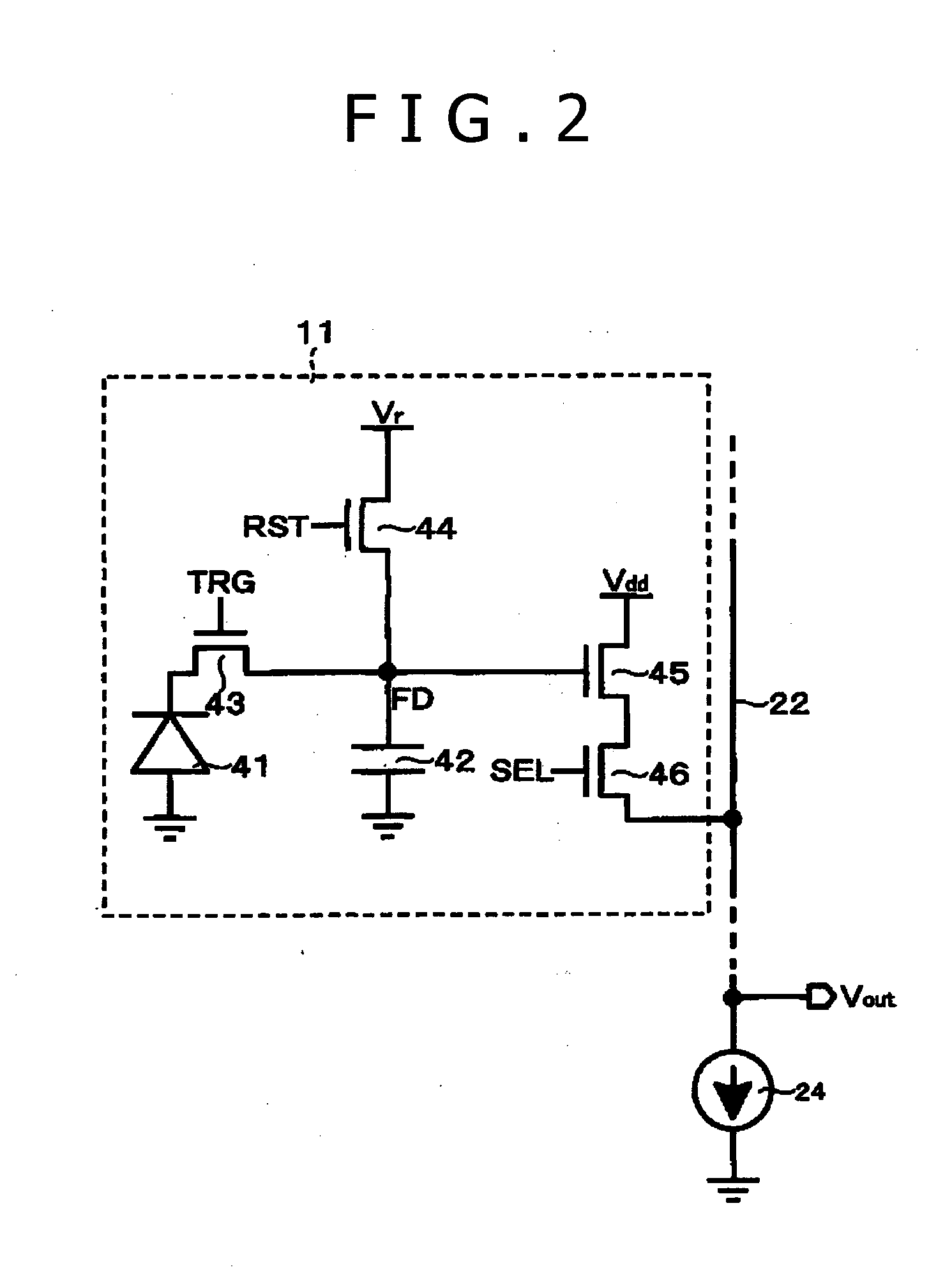
[0126]FIG. 15 is a timing waveform diagram for explaining a driving method according to working example 1. As shown in FIG. 15, in readout of the signal of the pixel on the i-th pixel row, the (i−1)-th pixel row, from which readout has been performed immediately before, is selected and the FD part 42 is reset to the reset potential Vr. Furthermore, the reset level Vrst—i−1 is read out and this reset level Vrst—i−1 is set as the reference voltage Vzr of the AD conversion circuit 23.
[0127]Subsequently, the i-th pixel row is selected and the signal level Vsig—i is read out to carry out AD conversion. Thereafter, the FD part 42 in the pixel on the i-th pixel row is reset to the reset potential Vr and the reset level Vrst—i is read out as the noise level to carry out AD conversion. In this AD conversion, denoising processing by correlated double sampling of subtracting the reset level Vrst—i from the signal level Vsig—i is executed.
[0128]The operation sequence of this correlated double s...
working example 2
[0135]FIG. 16 is a timing waveform diagram for explaining a driving method according to working example 2. The basic operation is the same as that of working example 1. The difference from working example 1 is omission of the operation of resetting the FD part 42 to the reset potential Vr in acquisition of the reference voltage of the AD conversion circuit 23.
[0136]In the pixel selected in order to acquire the reference voltage of the AD conversion circuit 23, the FD part 42 has been already reset to the reset potential Vr in order to read out the reset level after readout of the signal level. Therefore, the operation of resetting the FD part 42 in acquisition of the reference voltage can be omitted. This omission of the operation of resetting the FD part 42 in acquisition of the reference voltage of the AD conversion circuit 23 can enhance the operation speed.
[0137]However, if voltage variation over time is large due to a leakage current generated in the FD part 42 and so forth, wo...
PUM
 Abstract
Description
Claims
Application Information