Display device and electronic device using the same

a technology of electronic devices and display devices, applied in lighting devices, instruments, light sources, etc., can solve the problems of ineffective utilization of inability to easily reduce the driving voltage of pixels, and inability to effectively utilize driver ics with low output voltage. achieve the effect of low power consumption

Inactive Publication Date: 2012-03-08
INNOLUX CORP
View PDF6 Cites 130 Cited by
  • Summary
  • Abstract
  • Description
  • Claims
  • Application Information

AI Technical Summary

Benefits of technology

[0014]Therefore, a display device with low power consumption may be realized.

Problems solved by technology

Because of temperature, brightness, or other condition limitations, the pixel driving voltage cannot be easily lowered.
Even so, lowering the pixel driving voltage is still limited, such that a driver IC having a low output voltage cannot be effectively utilized in a display device.

Method used


Image

  • Display device and electronic device using the same
  • Display device and electronic device using the same
  • Display device and electronic device using the same

Examples


embodiment 1

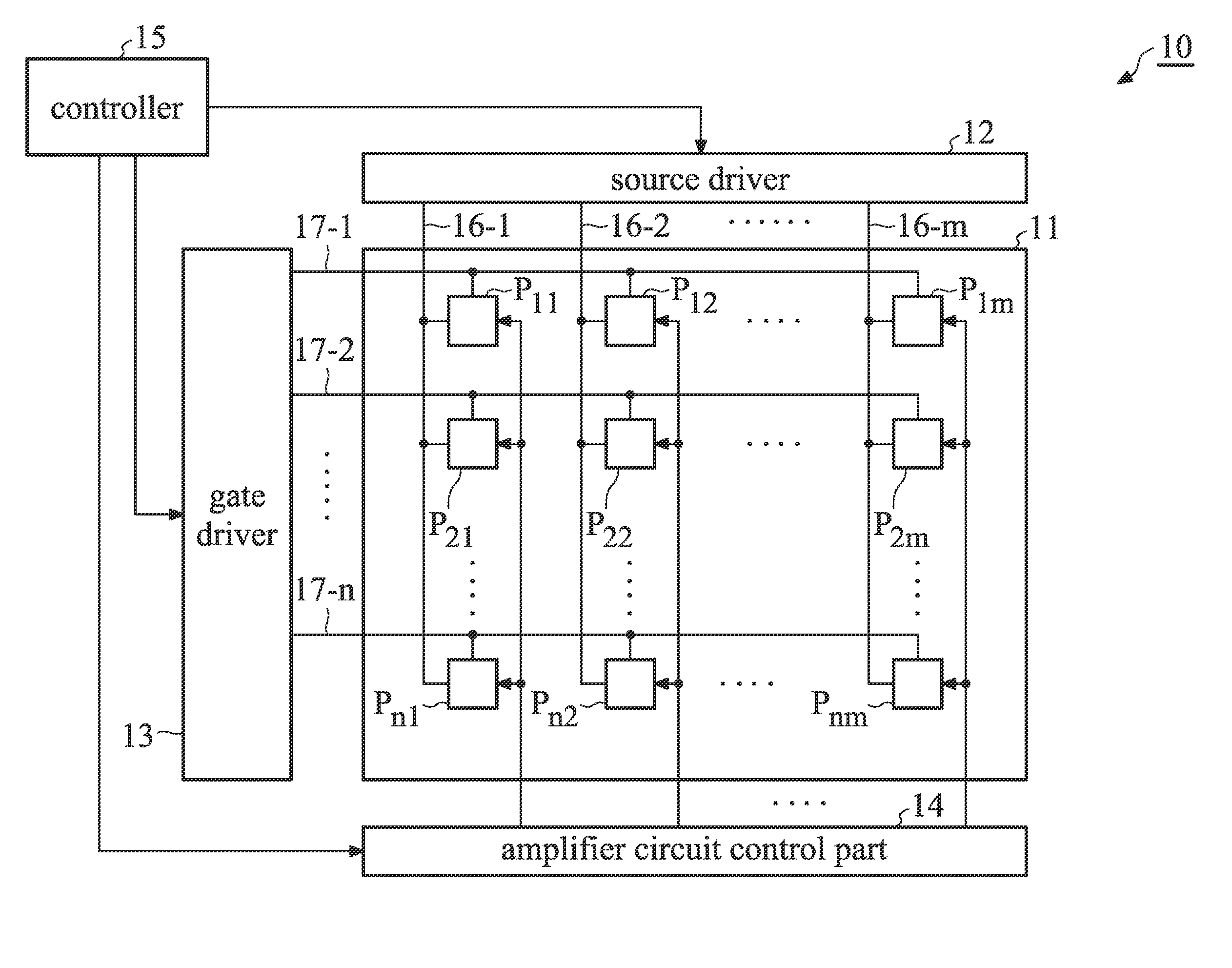
[0038]FIG. 1 is a block diagram of a display device in accordance with Embodiment 1 of the invention. In FIG. 1, a display device 10 comprises a display panel 11, a source driver 12, a gate driver 13, an amplifier circuit control part 14, and a controller 15.

[0039]The display panel 11 comprises a plurality of pixels P11˜Pnm (m and n are integers) arranged in a matrix formed by rows and columns. The display panel 11 further comprises a plurality of source lines 16-1˜16-m arranged corresponding to the columns, and a plurality of gate lines 17-1˜17-n arranged corresponding to the rows and orthogonal to the source lines 16-1˜16-m.

[0040]The source driver 12 generates signal voltages to the source lines 16-1˜16-m. The gate driver 13, via the gate lines 17-1˜17-n, controls signal voltage applications from the source lines 16-1˜16-m to the pixels P11˜Pnm. Specifically, the gate driver 13 drives pixel rows or columns (in FIG. 1, pixel rows are taken as an example) with an interlaced scan or ...

embodiment 2

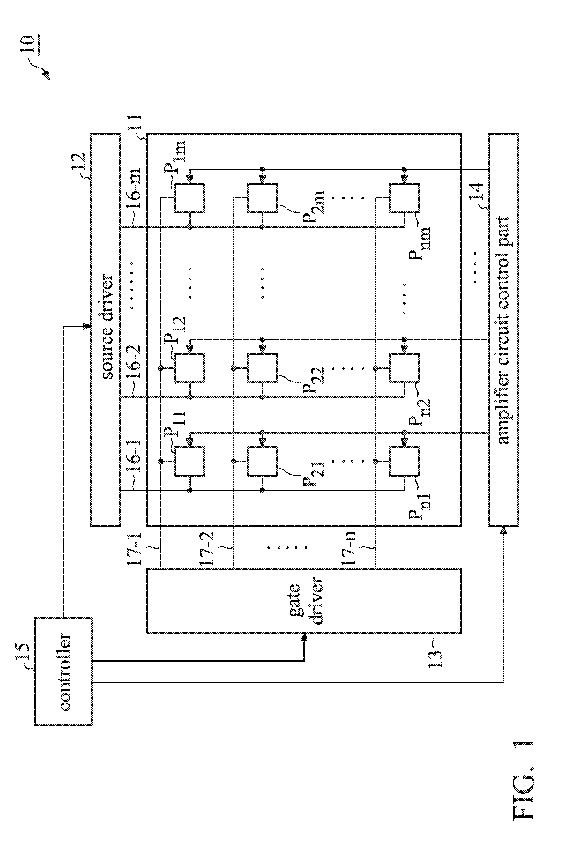
[0068]FIG. 8 is a block diagram of a display device in accordance with Embodiment 2 of the invention. In FIG. 8, a display device 80 comprises a display panel 11, a source driver 12, a gate driver 13, an amplifier circuit control part 14, and a controller 15.

[0069]In the display device 80 shown in FIG. 8, the amplifier circuit control part 14 controls amplifier circuits arranged on the source lines 16-1˜16-m between the source driver 12 and the pixel columns. Besides this, the display device 80 has the same structure as that of the display device 10 shown in FIG. 1.

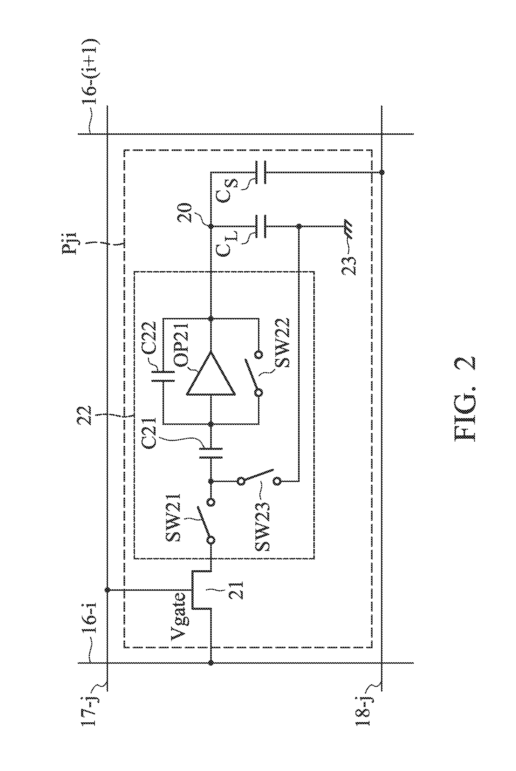
[0070]FIG. 9 is a circuitry diagram of an amplifier circuit arranged on each source line in the display device in accordance with Embodiment 2.

[0071]An amplifier circuit 90 is arranged on each source line between the source driver 12 and the pixel columns to amplify a signal voltage applied by the source driver 12 to the source line 16-i to a driving voltage capable of driving pixels connected to the source line 16-i. The...

embodiment 3

[0081]FIG. 11 is a block diagram of a display device in accordance with Embodiment 3 of the invention. In FIG. 11, a display device 110 comprises a display panel 11, a source driver 12, a gate driver 13, an amplifier circuit control part 14, and a controller 15.

[0082]The display device 110 shown in FIG. 11 further comprises capacity storage lines 18-1˜18-n arranged corresponding to the pixel rows and parallel to the gate lines 17-1˜17-n, and a capacity storage driver 19 driving the capacity storage lines 18-1˜18-n in synchronization with the driving of the pixels (namely, in synchronization with the operation where the gate driver 13 applies scan signals to the gate lines 17-1˜17-n). Besides this, the display device 110 shown in FIG. 11 has the same structure as that of the display device 10 shown in FIG. 1.

[0083]By the control of the controller 15, the capacity storage driver 19 drives the capacity storage lines 18-1˜18-n in synchronization with the gate lines 17-1˜17-n applied wit...


PUM


Abstract

The invention provides a low-power consumption display device. The display device 10 is provided with a plurality of pixels P11˜Pnm arranged in a matrix formed by columns and rows, and a plurality of signal lines 16-1˜16-m arranged corresponding to every pixel rows or pixel columns. The display device further comprises a signal voltage generating part 12 electrically connected to the plurality of pixels P11˜Pnm via the plurality of signal lines 16-1˜16-m and generating signal voltages which are applied to the plurality of signal lines 16-1˜16-m, and a signal voltage amplifying part 14 amplifying the signal voltage generated by the signal voltage generating part 12 to a necessary drive voltage for each of the plurality of pixels P11˜Pnm.

Description

CROSS REFERENCE TO RELATED APPLICATIONS[0001]This Application claims priority of Japanese Patent Application No. 2010-196467, filed on Sep. 2, 2010, the entirety of which is incorporated by reference herein.BACKGROUND OF THE INVENTION[0002]1. Field of the Invention[0003]The present invention relates to a display device having a plurality of pixels arranged in a matrix formed by rows and columns and a plurality of signal lines corresponding to the rows or the columns, and an electronic device using the same[0004]2. Description of the Related Art[0005]For a display device having a plurality of pixels arranged in a matrix formed by rows and columns, each pixel comprises a switch element provided at a cross region of a signal line (or called a source line) and a scan line (or called a gate line). Each pixel further comprises a pixel electrode formed on a substrate where the switch element is formed and a common electrode formed on an opposite substrate. The common electrode connects all...

Claims


Application Information

Patent Timeline
Patent Type & Authority Applications(United States)
IPC IPC(8): H05B37/02
CPCG09G3/3659G09G3/3688G09G2330/021G09G2300/0833G09G2300/0804
Inventor TOSHIYA, INADANAGAI, HAJIME
Owner INNOLUX CORP
Why Eureka
Try Eureka