Alignment Mark, Substrate, Set of Patterning Devices, and Device Manufacturing Method
a technology of alignment marks and substrates, applied in the direction of measurement devices, optics, instruments, etc., can solve the problem that the measurement techniques of different methods and tools cannot be (directly) compared, and achieve the effect of avoiding obscuring the purpos
- Summary
- Abstract
- Description
- Claims
- Application Information
AI Technical Summary
Benefits of technology
Problems solved by technology
Method used
Image
Examples
embodiment 1
[0092]2. The alignment mark of embodiment 1, wherein the at least one sub-mark is the first sub-mark or the second sub-mark.
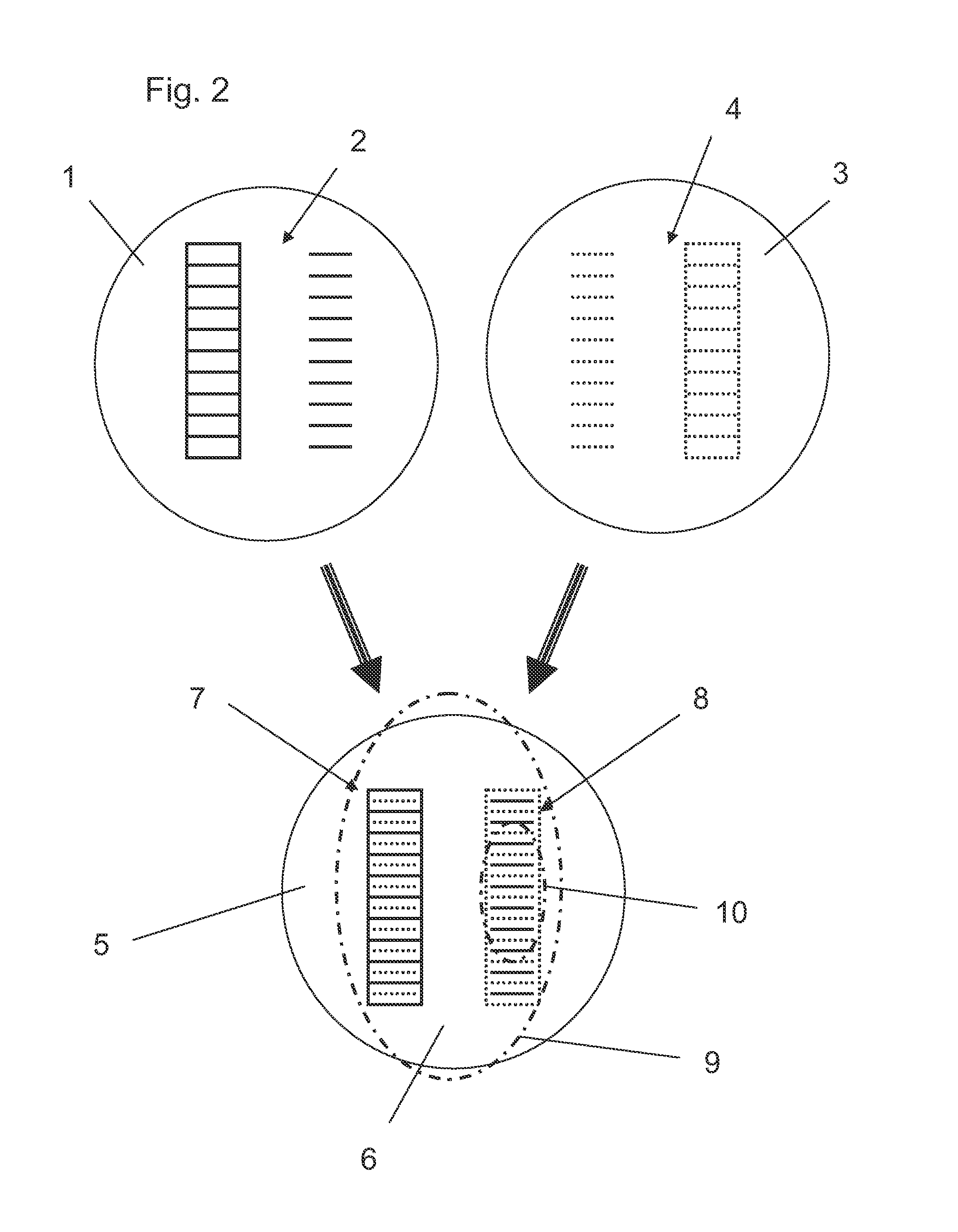
[0093]3. The alignment mark of embodiment 1, wherein each of the first sub-mark and the second sub-mark are defined by image lines of the first alignment pattern and the second alignment pattern.
[0094]4. The alignment mark of embodiment 1, wherein, in the at least one sub-mark, image lines of one of the first and second alignment pattern enclose lines of the other alignment pattern.
[0095]5. The alignment mark of embodiment 1, wherein, in the at least one sub-mark, image lines of one of the first and second alignment pattern define an array of rectangular cells, and lines of the other of the first and second alignment pattern define a line within each of the rectangular cells.
[0096]6. The alignment mark of embodiment 1, wherein the first exposure and the further exposure are part of a double patterning process.
[0097]7. The alignment mark of embodiment 1, wherein...
embodiment 15
[0114]16. The method of embodiment 15, wherein the first and further exposure are part of a double patterning process.
[0115]17. The method of embodiment 15, wherein the alignment mark comprises any of the features of the embodiments 1-11.
[0116]19. The method of embodiment 15, wherein a photo-resistive layer is arranged on the substrate between the first and further exposure.
[0117]Although specific reference may be made in this text to the use of lithographic apparatus in the manufacture of ICs, it should be understood that the lithographic apparatus described herein may have other applications, such as the manufacture of integrated optical systems, guidance and detection patterns for magnetic domain memories, flat-panel displays, liquid-crystal displays (LCDs), thin-film magnetic heads, etc. The skilled artisan will appreciate that, in the context of such alternative applications, any use of the terms “wafer” or “die” herein may be considered as synonymous with the more general term...
PUM
| Property | Measurement | Unit |
|---|---|---|
| thickness | aaaaa | aaaaa |
| thickness | aaaaa | aaaaa |
| size | aaaaa | aaaaa |
Abstract
Description
Claims
Application Information


