Connector, cable assembly, and semiconductor testing device

a technology of connecting cable and connector, which is applied in the direction of coupling device connection, contact member penetrating/cutting insulation/cable strand, instruments, etc., can solve the problems of signal transmission characteristics deterioration, difficult coaxial structure of signal terminal and ground terminal, etc., to achieve easy inserting and pulling out the connector, and easy to insert and pull out the connector

Active Publication Date: 2012-04-19
ADVANTEST CORP
View PDF3 Cites 10 Cited by
  • Summary
  • Abstract
  • Description
  • Claims
  • Application Information

AI Technical Summary

Benefits of technology

[0016]Further, according to an aspect of the present invention, the enclosure includes an extended portion, which extends in an insertion / pulling-out direction of the connector from a periphery of an opening-forming surface in which an opening of the insertion hole is formed, and which forms a recessed portion including the opening-forming surface as a bottom surface of the recessed portion. As a result, it becomes easy to insert and pull out the connector.
[0017]Further, according to an aspect of the present invention, a tip end portion of the extended portion is provided with a flange portion projecting in an outward direction of the opening-forming surface. As a result, it becomes even easier to insert and pull out the connector.
[0018]Further, according to an aspect of the present invention, when the connector serving as a male connector fits into a female connector serving as a counterpart for the male connector, the extended portion is positioned outside the female connector. In this way, it becomes still easier to insert and pull out the connector. Further, according to the present invention, there is provided a semiconductor testing device including the above-mentioned cable assembly according to the present invention.

Problems solved by technology

However, due to needs for reduction in space or the like, it may sometimes be difficult for the signal terminal and the ground terminal to have the coaxial structure.
Therefore, there is a fear that signal transmission characteristics may be deteriorated.

Method used


Image

  • Connector, cable assembly, and semiconductor testing device
  • Connector, cable assembly, and semiconductor testing device
  • Connector, cable assembly, and semiconductor testing device

Examples


Embodiment Construction

[0033]A connector, a cable assembly, and a semiconductor testing device according to an embodiment of the present invention are described with reference to the drawings.

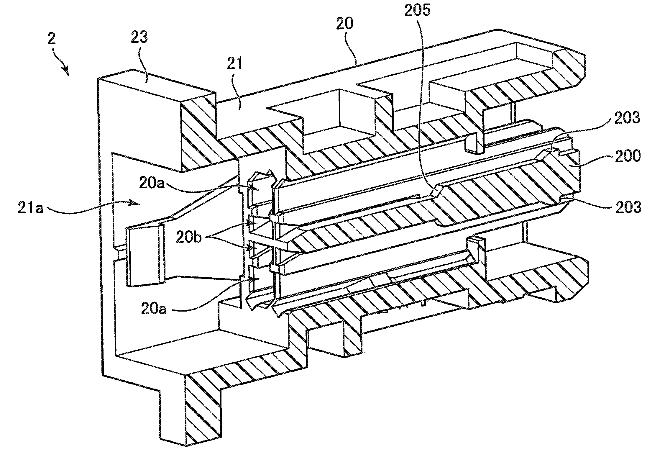
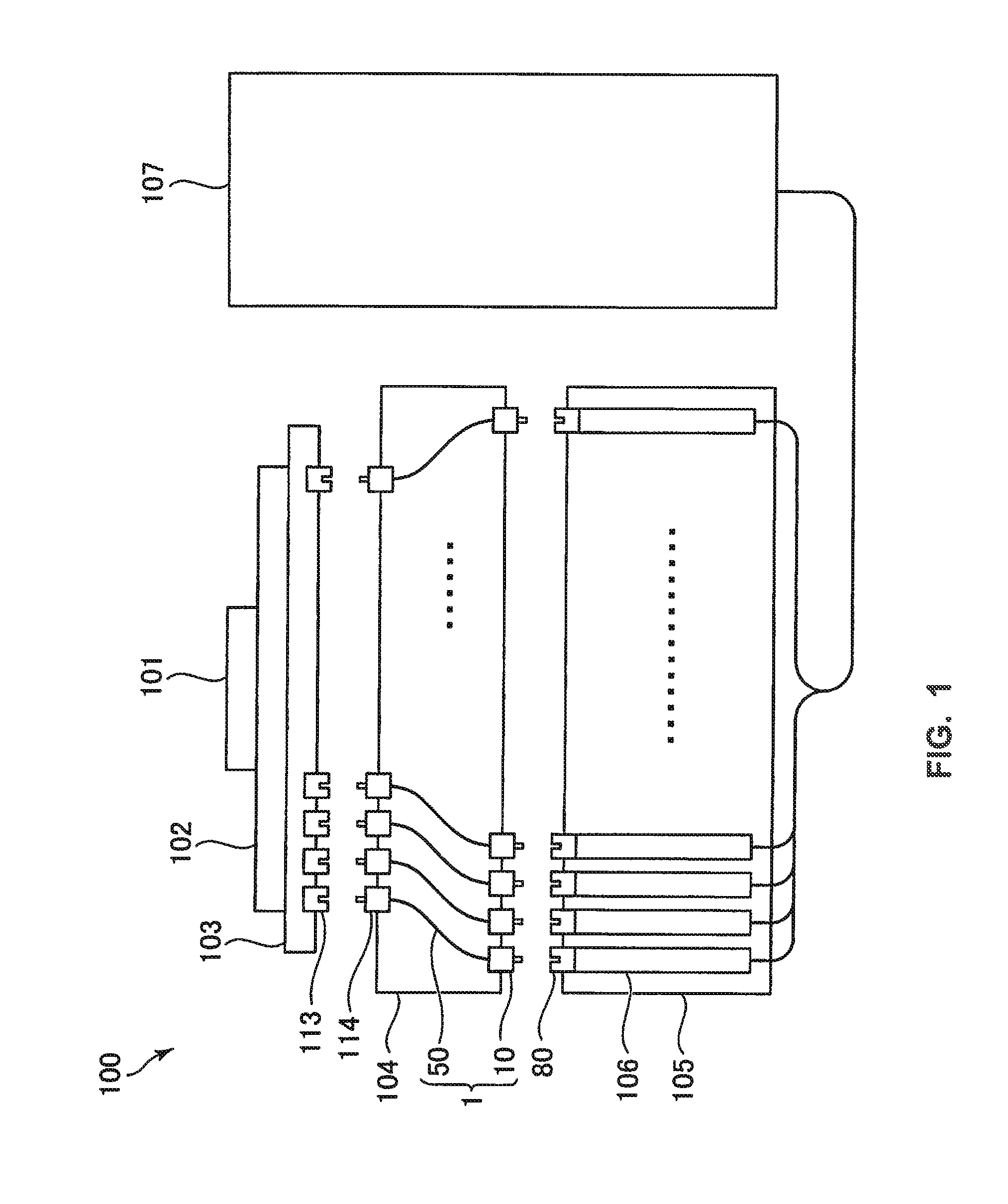
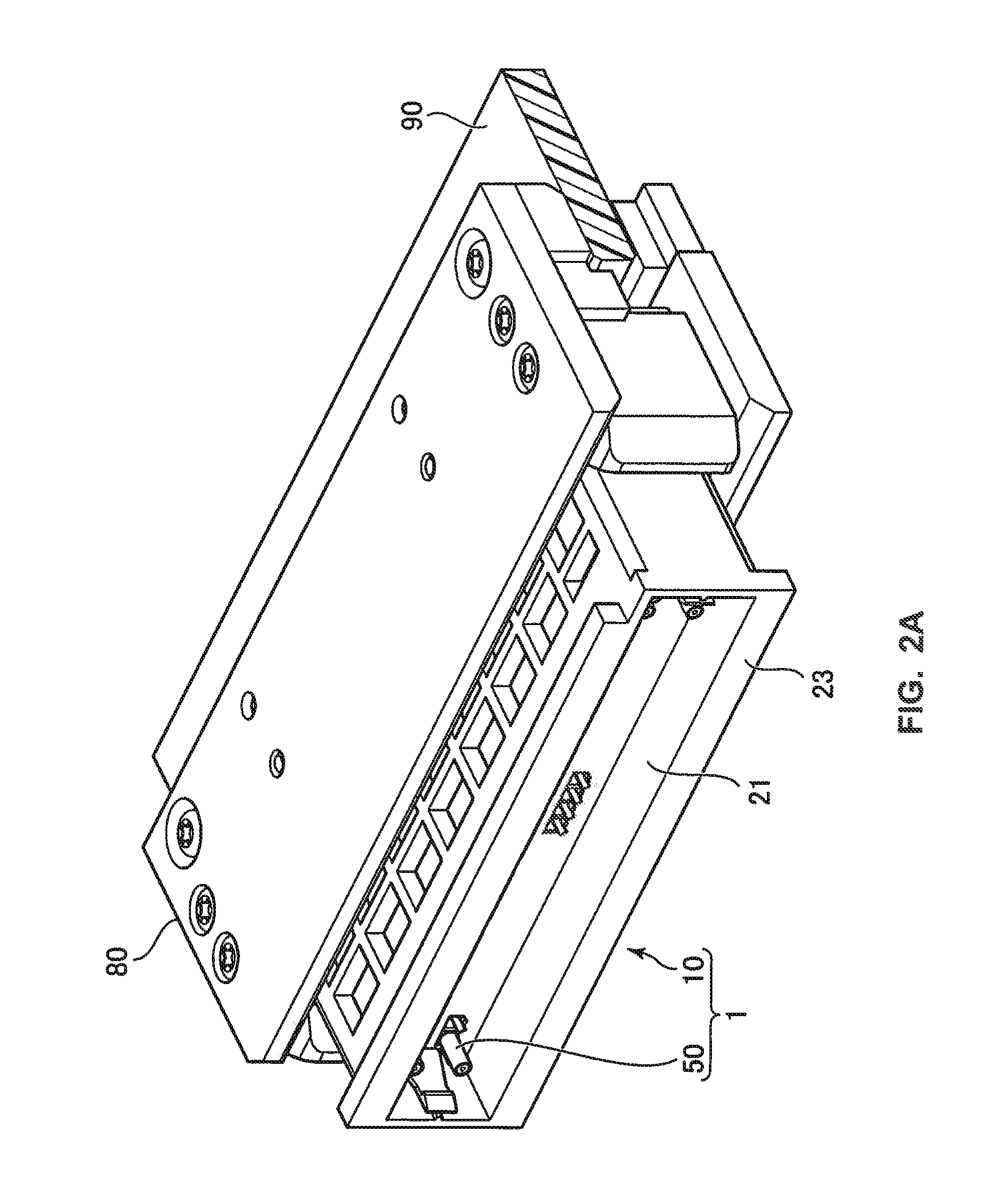
[0034]FIG. 1 is a schematic view of a semiconductor testing device 100 according to an embodiment of the present invention. The semiconductor testing device 100 includes: a test head 105; a mother board 104 to be arranged above the test head 105; a performance board 103 to be arranged above the mother board 104; and a device socket 102 to be arranged above the performance board 103.

[0035]A semiconductor 101 to be tested is mounted on the device socket 102. In a lower surface of the performance board 103, there are provided a plurality of connectors 113. Each of the connectors 113 is electrically connected to the semiconductor 101 through the performance board 103 and the device socket 102.

[0036]In an upper surface of the mother board 104, there are provided a plurality of connectors 114. Into each of the connectors 1...


PUM


Abstract

The connector includes an enclosure including insertion holes formed therein, into which tip end portions of coaxial cables provided with signal terminals and with ground terminals arranged at parts of peripheries of the signal terminals are inserted, and auxiliary ground conductors, which are retained by the enclosure, are electrically connected to the ground terminals, and are arranged at other parts of the peripheries of the signal terminals.

Description

FIELD OF THE INVENTION[0001]The present invention relates to a connector, a cable assembly, and a semiconductor testing device. In particular, the present invention relates to technology for achieving enhancement of signal transmission characteristics.BACKGROUND OF THE INVENTION[0002]Conventionally, there has been known a connector which allows a coaxial cable to be inserted therein so as to electrically connect the coaxial cable and electrical equipment. In the above-mentioned coaxial cable, there is provided a ground conductor surrounding a signal line. The ground conductor shields electromagnetic waves from the exterior.SUMMARY OF THE INVENTION[0003]A tip end portion of the coaxial cable is provided with a signal terminal and a ground terminal. The signal terminal and the ground terminal are connected to the signal line and the ground conductor, and serve to contact with counterpart terminals, respectively. In the above-mentioned tip end portion, also, it is preferred to employ a...

Claims


Application Information

Patent Timeline
Patent Type & Authority Applications(United States)
IPC IPC(8): H01R9/05
CPCG01R31/2851H01R9/038H01R12/721H01R2201/20H01R9/0527H01R13/65918H01R4/24H01R24/30
Inventor MOTOHASHI, NOBUMASAMIZUMURA, AKIONORINIITSU, TOSHIHIROSUZUKI, TERUHITOSAKIYAMA, SHIN
Owner ADVANTEST CORP
Why Eureka
Try Eureka