

Wafer level semiconductor package and manufacturing methods thereof
a technology of semiconductor packages and manufacturing methods, applied in the direction of semiconductor devices, semiconductor/solid-state device details, electrical apparatus, etc., can solve the problems of increased process complexity and cost, contact pads occupying a significant amount of the surface area of semiconductor packages, and semiconductor devices becoming progressively more complex
- Summary
- Abstract
- Description
- Claims
- Application Information
AI Technical Summary
Benefits of technology
Problems solved by technology
Method used
Image

Examples
Embodiment Construction
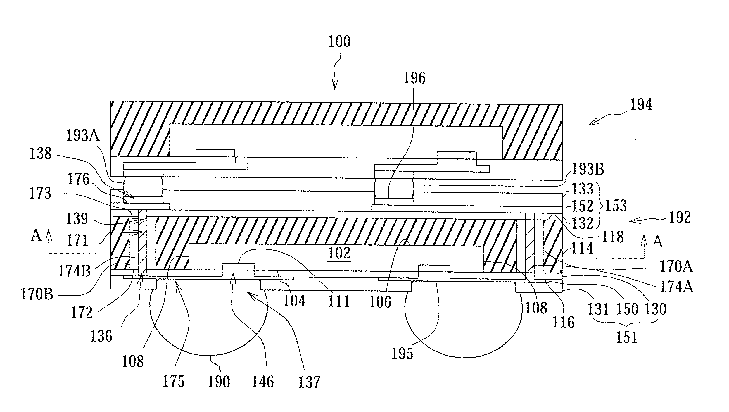
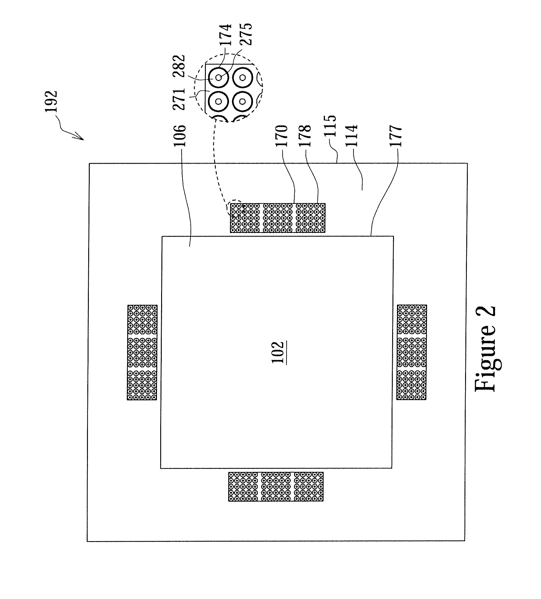
[0020]Referring to FIG. 1, a cross section view is shown of a stacked package assembly 100 according to an embodiment of the invention. The stacked package assembly 100 includes a semiconductor package 192 and a semiconductor package 194 positioned above the semiconductor package 192. The semiconductor package 194 is electrically connected to the semiconductor package 192 through conductive bumps 193. It is contemplated that the semiconductor package 194 may be any form of semiconductor package, such as a wafer-level package, a BGA package, and a substrate-level package. The semiconductor package 194 may also include a combination of one or more semiconductor packages and / or one or more passive electrical components. The semiconductor package 192 includes a semiconductor device 102, which includes a lower surface 104 which in the illustrated embodiment is an active surface, i.e. the active surface having die bond pads 111, an upper surface 106, and lateral surfaces 108 disposed adja...
PUM
 Abstract
Description
Claims
Application Information