Modified shield design to eliminate the far-field WATE problem
- Summary
- Abstract
- Description
- Claims
- Application Information
AI Technical Summary
Benefits of technology
Problems solved by technology
Method used
Image

Examples
first embodiment
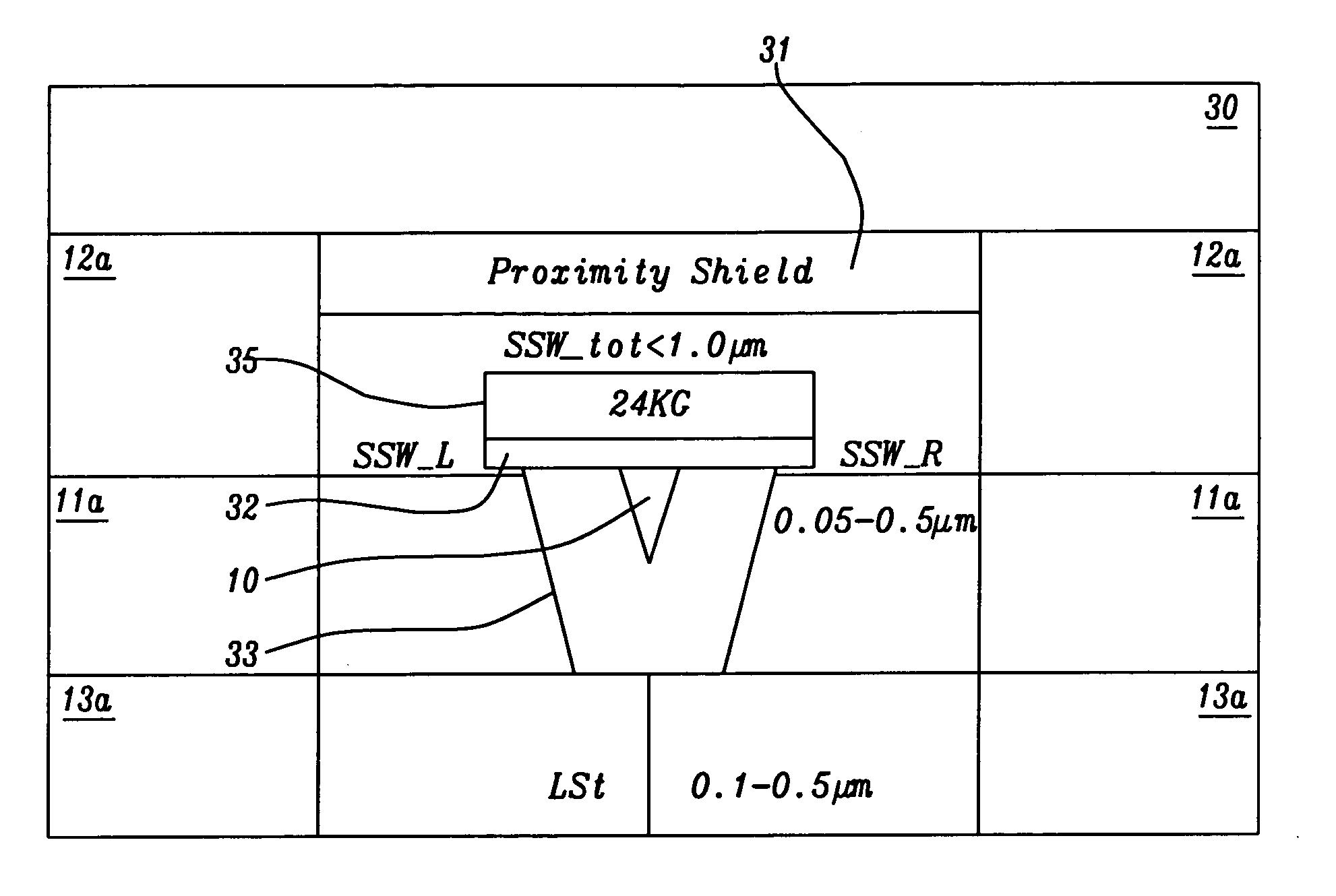
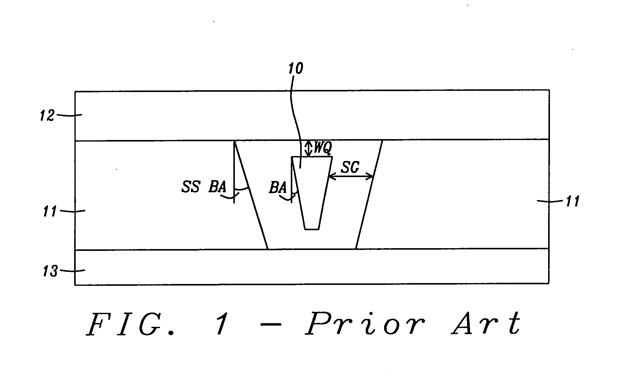
[0032]the invention (PSD#1 shown in FIGS. 3a and 3b) has a straight proximity shield with non-recessed top. FIG. 3b is a cross-section made in a plane normal to the ABS and showing recessed depth 34 as well as proximity shield 31, seed layer 35, write gap 32, main pole 10 side shield 11a, and leading shield 13a.
[0033]PSD#2, shown in FIGS. 4a and 4b has its top yoke recessed as well as LS, SS, and WS.
[0034]PSD#3, shown in ABS view in FIG. 5a, has a non-recessed central section 5b and recessed outer sections 5c in a similar manner to LS, SS, and WS.
[0035]PSD#4, shown in ABS view in FIG. 6a, has the proximity shields in the LS and SS regions conforming to the shape of the side and write gaps. An important feature of this design is that the magnetization of the proximity shield in the LS and SS regions is aligned to the edges of the side gap, as indicated by the arrows. This layout of the magnetization has the advantage of being an effective shield to reduce side fringing while continu...
PUM
 Abstract
Description
Claims
Application Information