Semiconductor defect classifying method, semiconductor defect classifying apparatus, and semiconductor defect classifying program

a technology of semiconductor defect and defect classification, applied in the field of semiconductor defect classification method, semiconductor defect classification apparatus, semiconductor defect classification program, can solve the problems of increasing the proportion of design-layout-dependent defects, systematic defects, layout-dependent defects, etc., and achieves rapid increase in the yield of semiconductor devices. , the effect of efficient and effective defect classification

Active Publication Date: 2012-05-24
HITACHI HIGH-TECH CORP
View PDF3 Cites 44 Cited by
  • Summary
  • Abstract
  • Description
  • Claims
  • Application Information

AI Technical Summary

Benefits of technology

[0021]According to the present invention, accurate determination of the state of overlap between a design layout pattern and a defect (within a pattern / over one or more patterns / outside a pattern) allows efficient and effective classification of defects and, additionally, identification of a systematic defect that is a problem for modern microdevices. Classification of such systematic defects leads to development and trial manufacture of semiconductor devices and rapid increase in the yield of semiconductor devices in mass production.

Problems solved by technology

However, in recent years, the minimum pattern line widths of semiconductor devices have been decreasing from 45 nm to 32 nm, and the proportion of design-layout-dependent defects is increasing.
Such a layout-dependent defect is called a systematic defect.
Examples of a systematic defect include an abnormality in resistance caused by a variation in pattern shape resulting from a difference in level of an underlayer and faulty electrical continuity of a contact hole caused by insufficient etching at a specific region of a gate oxide film.
However, the conventional ADC classification remains within classification into categories based on the shape, brightness, and the like of a defect observed with a review apparatus and cannot identify the cause of a layout-induced systematic defect.

Method used


Image

  • Semiconductor defect classifying method, semiconductor defect classifying apparatus, and semiconductor defect classifying program
  • Semiconductor defect classifying method, semiconductor defect classifying apparatus, and semiconductor defect classifying program
  • Semiconductor defect classifying method, semiconductor defect classifying apparatus, and semiconductor defect classifying program

Examples


Embodiment Construction

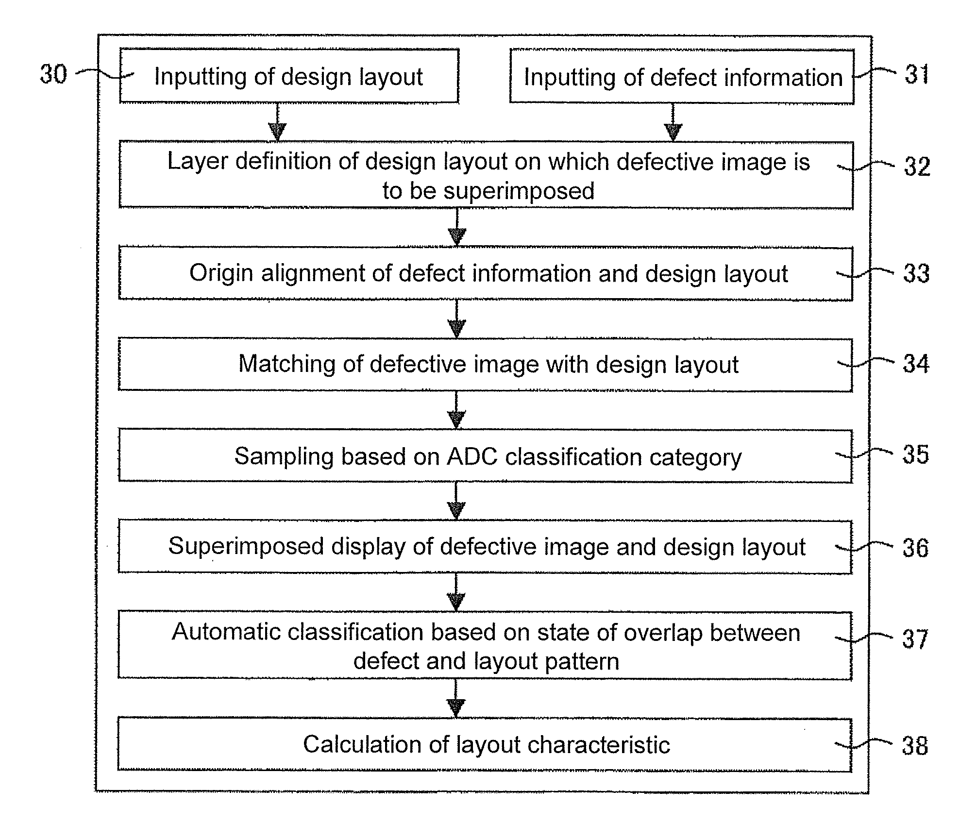
[0032]An embodiment of the present invention will be described below with reference to the drawings.

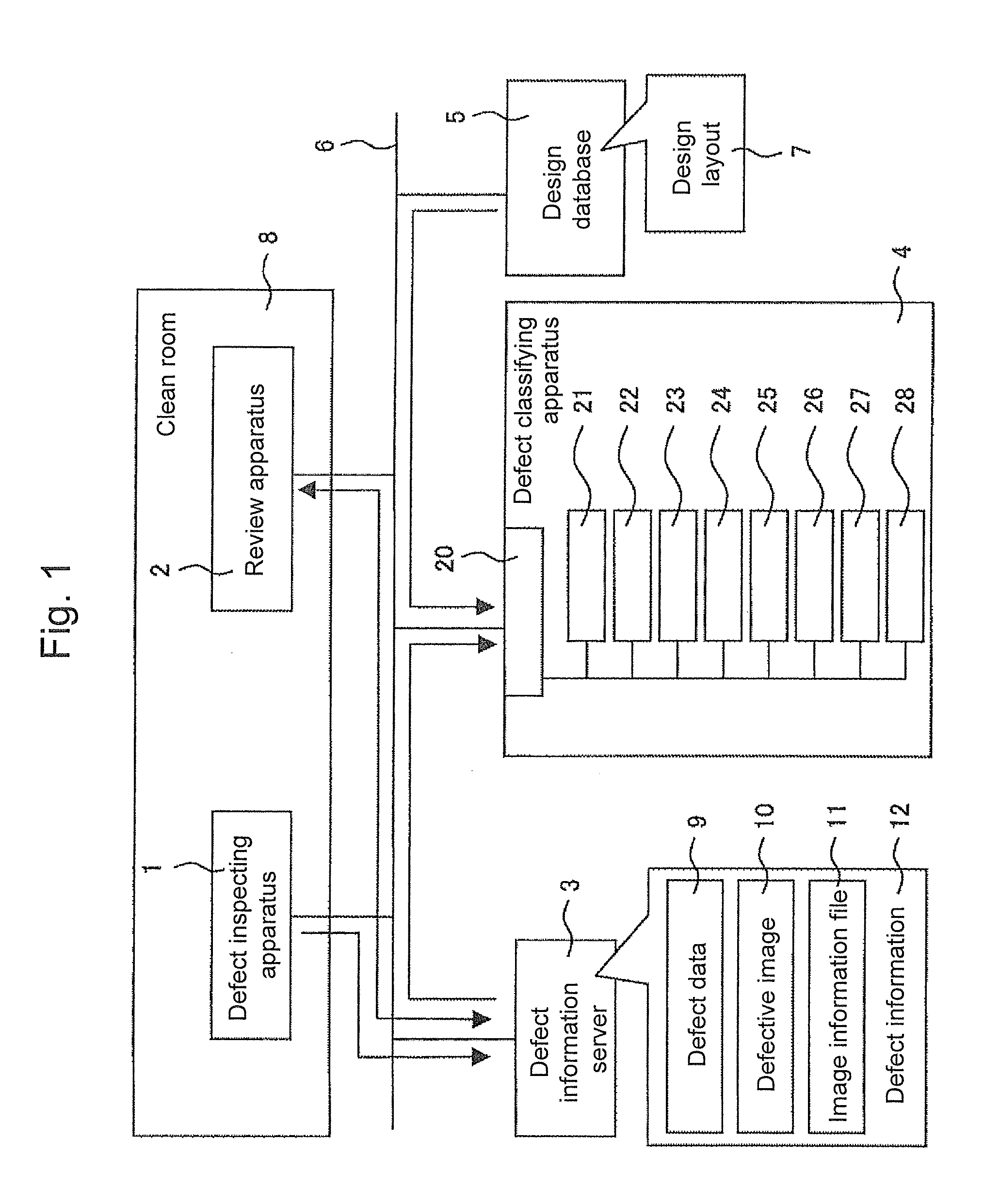
[0033]The overall configuration of the present invention will be described with reference to FIG. 1. A semiconductor manufacturing process is generally performed in a clean room 8 in an environment kept clean. A defect inspecting apparatus 1 which inspects a finished wafer for defects is placed in the clean room 8. The defect inspecting apparatus 1 is, e.g., a dark-field defect inspecting apparatus, a bright-field defect inspecting apparatus, or an electron-beam defect inspecting apparatus. The defect inspecting apparatus 1 may have the function of detecting a defect appearing at the surface of a device to be inspected and simultaneously acquiring a review image of the detected defect (a defective image 10). A review apparatus 2 which observes a defect detected by the defect inspecting apparatus 1 on the basis of the coordinate information of the defect is placed in the clean room 8. ...


PUM


Abstract

A defect is efficiently and effectively classified by accurately determining the state of overlap between a design layout pattern and the defect. This leads to simple identification of a systematic defect. A defective image obtained through defect inspection or review of a semiconductor device is automatically pattern-matched with design layout data. A defect is superimposed on a design layout pattern for at least one layer of a target layer, a layer immediately above the target layer, and a layer immediately below the target layer. The state of overlap of the defect is determined as within the pattern, over the pattern, or outside the pattern, and the defect is automatically classified.

Description

TECHNICAL FIELD[0001]The present invention relates to a semiconductor defect classifying method, a semiconductor defect classifying apparatus, a program for a semiconductor defect classifying apparatus, a semiconductor defect inspecting method, and a semiconductor defect inspecting system for classifying defects including a systematic defect in a wafer or chip during a semiconductor device manufacturing process.BACKGROUND ART[0002]The major cause of reduction in wafer fabrication yield in the pre-process of semiconductor manufacturing has conventionally been a foreign matter appearing randomly on a semiconductor wafer, and the yield has been maintained by reducing foreign matters. However, in recent years, the minimum pattern line widths of semiconductor devices have been decreasing from 45 nm to 32 nm, and the proportion of design-layout-dependent defects is increasing.[0003]Such a layout-dependent defect is called a systematic defect. Examples of a systematic defect include an abn...

Claims


Application Information

Patent Timeline
Patent Type & Authority Applications(United States)
IPC IPC(8): G06F17/50
CPCG01N21/95607G01N21/8851
Inventor HAYAKAWA, KOICHIHIRAI, TAKEHIROTANDAI, YUTAKAISHIKAWA, TAMAOSAKAI, TSUNEHIROHASUMI, KAZUHISANEMOTO, KAZUNORIICHINOSE, KATSUHIKOTAKAGI, YUJI
Owner HITACHI HIGH-TECH CORP
Why Eureka
Try Eureka