

System and method for scan testing integrated circuits
a technology of integrated circuit and scan test, which is applied in the field of integrated circuit testing, can solve the problems of increasing circuit density, difficult circuit testing, and high cost, and achieves the effects of increasing the density of circuits, reducing the cost of testing, and increasing the cost of testing
- Summary
- Abstract
- Description
- Claims
- Application Information
AI Technical Summary
Problems solved by technology
Method used
Image

Examples
Embodiment Construction
[0016]The detailed description of the appended drawings is intended as a description of the currently preferred embodiments of the present invention, and is not intended to represent the only form in which the present invention may be practiced. It is to be understood that the same or equivalent functions may be accomplished by different embodiments that are intended to be encompassed within the spirit and scope of the present invention.
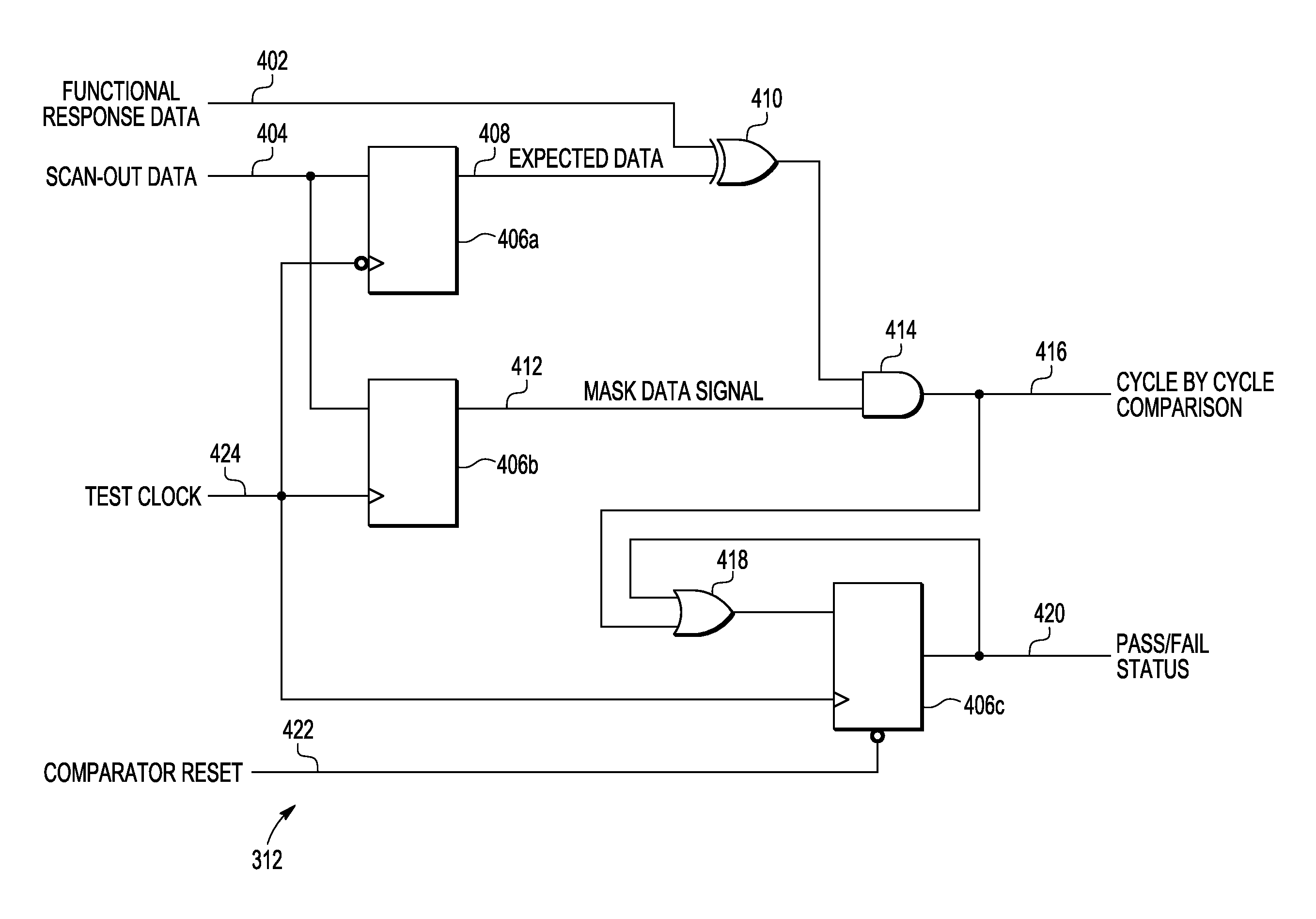
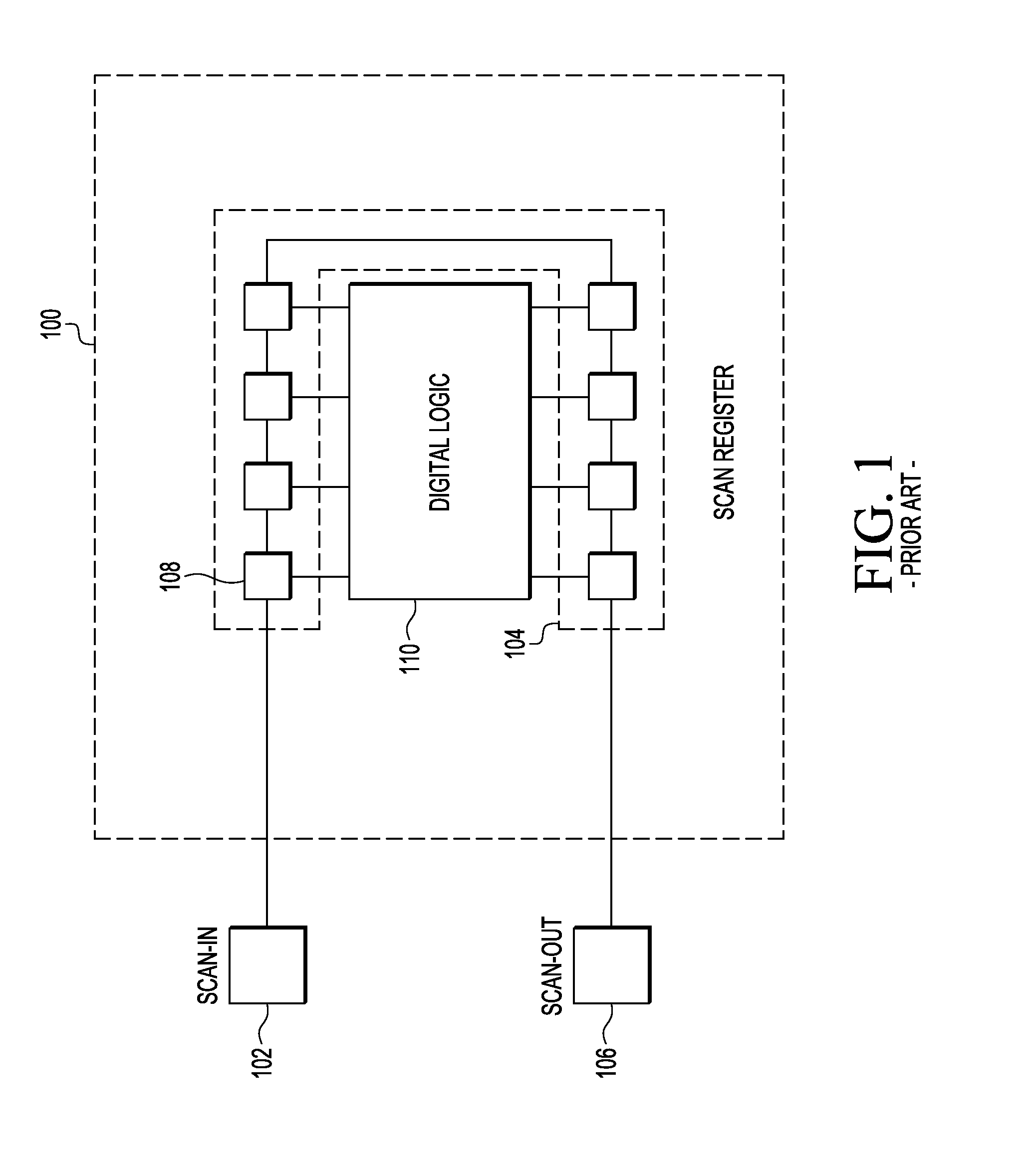
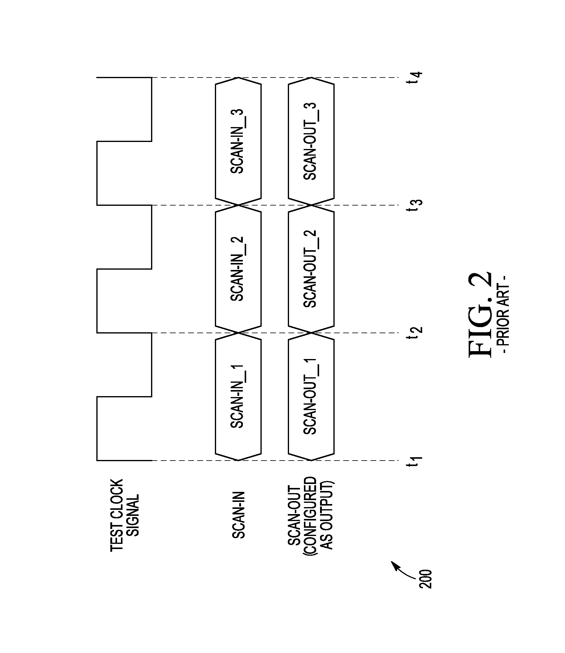
[0017]In an embodiment of present invention, a system for testing an integrated circuit is provided. The system includes one or more scan-in pads connected to one or more scan cells. The one or more scan cells are configured as a shift register. The shift register so formed is known as scan register. Further, one or more scan-out pads are connected to the one or more scan cells. Further, one or more comparators are connected to the one or more scan-out pads and one or more scan registers in the IC. Scan test data is transmitted from the one or more s...
PUM
 Abstract
Description
Claims
Application Information