
Printed circuit board and method of manufacturing the same

Inactive Publication Date: 2012-06-07
SAMSUNG ELECTRO MECHANICS CO LTD
View PDF15 Cites 29 Cited by
  • Summary
  • Abstract
  • Description
  • Claims
  • Application Information

AI Technical Summary

Benefits of technology

[0015]Accordingly, the present invention has been made keeping in mind the problems encountered in the related art and the present invention is intended to provide a PCB and a method of manufacturing the same, in which the contact area between a circuit pattern and an insulating layer may be increased thus solving separation problems of the circuit pattern, minimizing damage to the circuit pattern due to undercutting, and achieving a fine circuit pattern.

Problems solved by technology

However, the circuit pattern resulting from such SAP has the following problems.
Specifically, the force of adhesion between the circuit pattern and the insulating layer becomes problematic.
Because the circuit pattern having metallic properties and the insulating layer having insulating properties are formed of materials that are different from each other, the adhesion therebetween is limited.
However, when a fine circuit pattern is formed, the contact area between the circuit pattern and the insulating layer is remarkably reduced, unfortunately easily allowing the circuit pattern to separate from the surface of the insulating layer.
Furthermore, in the course of etching and removing the seed layer exposed from the circuit pattern formed using electroplating, undercut defects may occur in the circuit pattern.
Furthermore, the resolution of the fine circuit pattern becomes problematic.

Method used


Image

  • Printed circuit board and method of manufacturing the same
  • Printed circuit board and method of manufacturing the same
  • Printed circuit board and method of manufacturing the same

Examples


Embodiment Construction

[0034]Hereinafter, embodiments of the present invention will be described in detail while referring to the accompanying drawings. Throughout the drawings, the same reference numerals are used to refer to the same or similar constituents. Furthermore, descriptions of known techniques, even if they are pertinent to the present invention, are regarded as unnecessary and may be omitted in so far as they would make the characteristics of the invention unclear.

[0035]Furthermore, the terms and words used in the present specification and claims should not be interpreted as being limited to typical meanings or dictionary definitions, but should be interpreted as having meanings and concepts relevant to the technical scope of the present invention based on the rule according to which an inventor can appropriately define the concept implied by the term to best describe the method he or she knows for carrying out the invention.

[0036]PCB

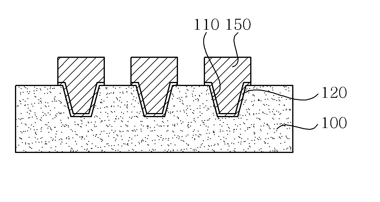
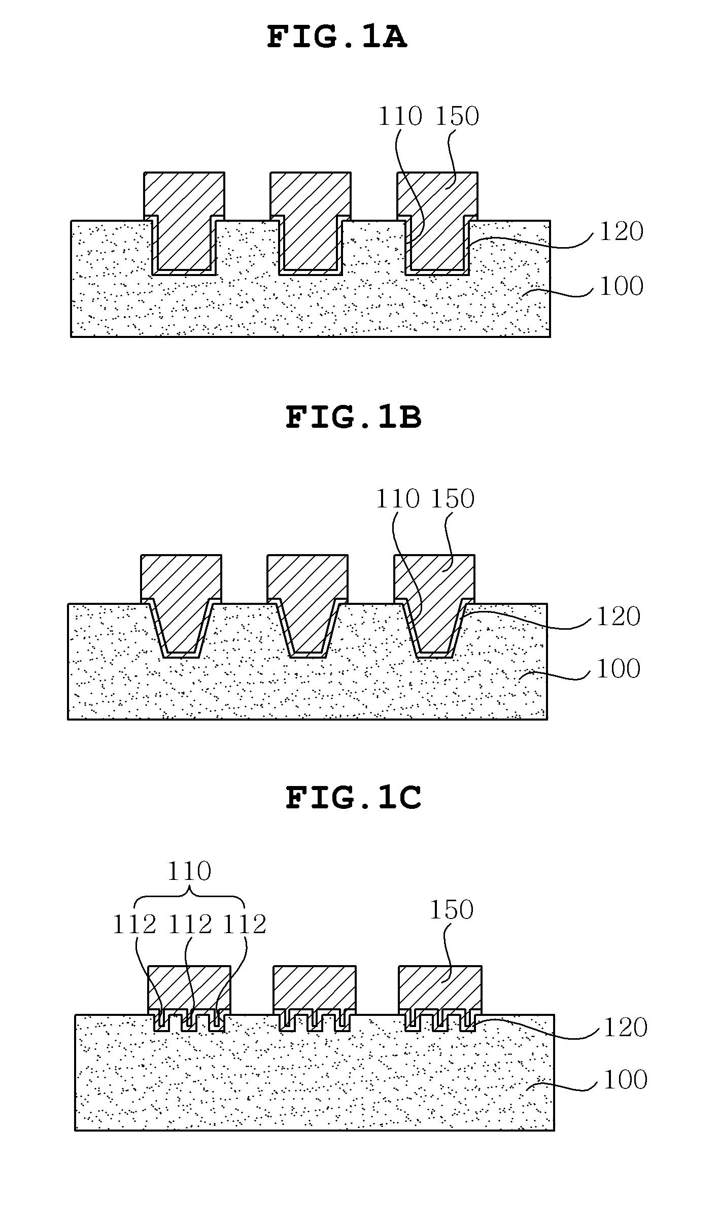
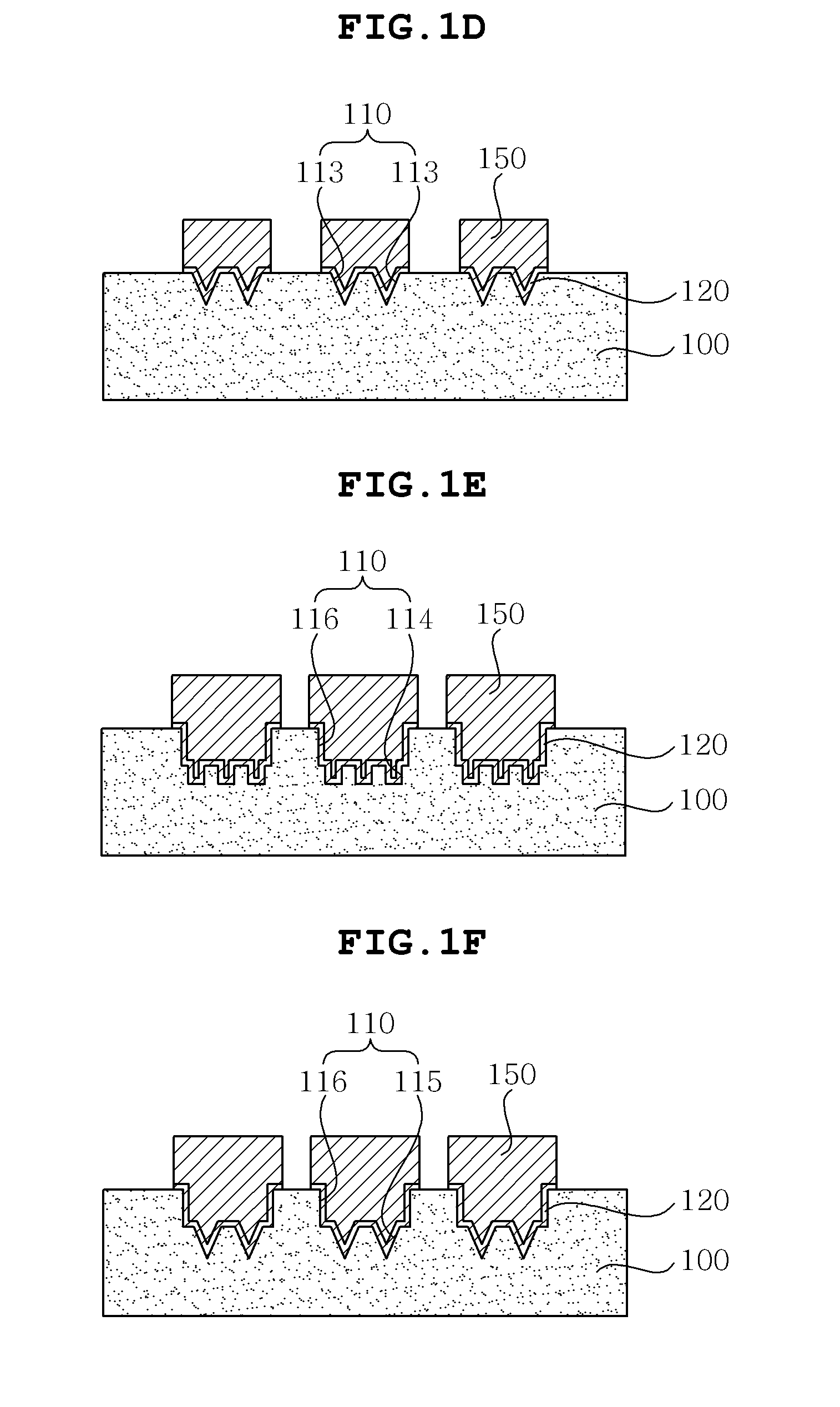
[0037]FIGS. 1A to 1F are cross-sectional views showing a PC...


PUM

PropertyMeasurementUnit
Adhesion strengthaaaaaaaaaa
aaaaaaaaaa

Abstract

Disclosed herein is a printed circuit board and a method of manufacturing the same, in which a circuit pattern one end of which is embedded in a trench and the other end of which protrudes from an insulating layer is formed, so that the circuit pattern is not easily separated from the insulating layer and the separation problems of the circuit pattern due to undercutting are solved. Also, the adhesion between the insulating layer and the circuit pattern is enhanced, more stably forming a fine circuit pattern. Even when a plating resist is formed thin, it is possible to form the circuit pattern, resulting in a high-solution circuit pattern.

Description

CROSS REFERENCE TO RELATED APPLICATION[0001]This application claims the benefit of Korean Patent Application No. 10-2010-0123705, filed Dec. 6, 2010, entitled “Printed circuit board and method of manufacturing the same”, which is hereby incorporated by reference in its entirety into this application.BACKGROUND OF THE INVENTION[0002]1. Technical Field[0003]The present invention relates to a printed circuit board (PCB) and a method of manufacturing the same.[0004]2. Description of the Related Art[0005]Mobile electronic devices including mobile phones, digital cameras and so on have recently made progress. This progress has been accompanied by ongoing research and development into smaller, slimmer and multi-functionalized electronic devices. Such a trend is directly linked with the demand to reduce the size of a semiconductor package which forms the electronic device, and it is ultimately required to increase the density of a substrate of the semiconductor package. Such a high-density ...

Claims


Application Information

Patent Timeline
IPC IPC(8): H05K1/02B05D5/12
CPCH05K3/107H01L2224/05557H05K3/381H05K3/108
Inventor WATANABE, RYOICHIKIM, GOING SIKRYU, CHANG SUP
Owner SAMSUNG ELECTRO MECHANICS CO LTD
Features
  • Generate Ideas
  • Intellectual Property
  • Life Sciences
  • Materials
  • Tech Scout
  • Unparalleled Data Quality
  • Higher Quality Content
  • 60% Fewer Hallucinations
Learn More