Pixel structure and manufacturing method thereof

a technology of pixel structure and manufacturing method, which is applied in the direction of electrical equipment, semiconductor devices, instruments, etc., can solve the problems of additional power consumption, and achieve the effect of maintaining the aperture ratio

Active Publication Date: 2012-06-07
AU OPTRONICS CORP
View PDF4 Cites 74 Cited by
  • Summary
  • Abstract
  • Description
  • Claims
  • Application Information

AI Technical Summary

Benefits of technology

[0008]The invention is directed to a pixel structure that includes a storage capacitor and can maintain the aperture ratio.
[0024]Based on the above, the pixel structure described herein is different from the conventional pixel structure because the electrode of the storage capacitor and the active layer can be made of the same material when the active layer is formed. Here, the material of the electrode and the active layer can be an oxide semiconductor material with high transmittance. As such, a stable display frame of the pixel structure can be provided by the storage capacitor, an aperture ratio of the pixel structure can be improved, and power consumption can be further reduced.

Problems solved by technology

When the pixel structure 100 is applied to a transmissive LCD, the light emission efficacy of the backlight source needs to be improved for maintaining the display luminance to some extent, which leads to additional power consumption.

Method used


Image

  • Pixel structure and manufacturing method thereof
  • Pixel structure and manufacturing method thereof
  • Pixel structure and manufacturing method thereof

Examples


Embodiment Construction

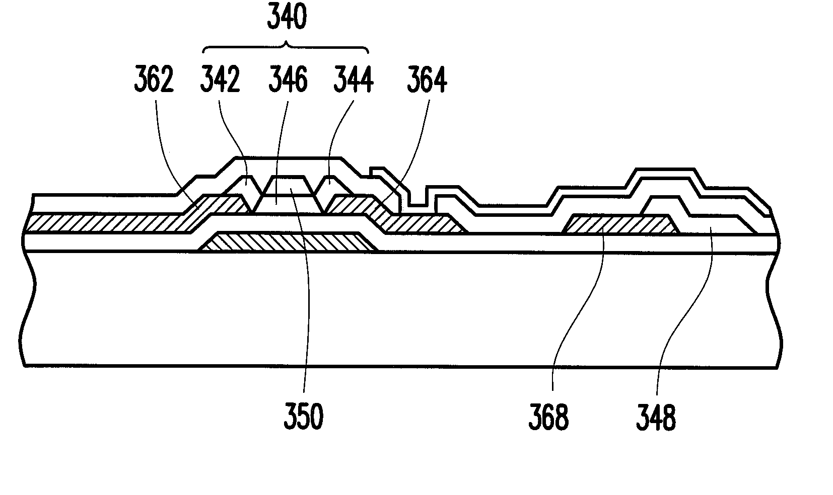
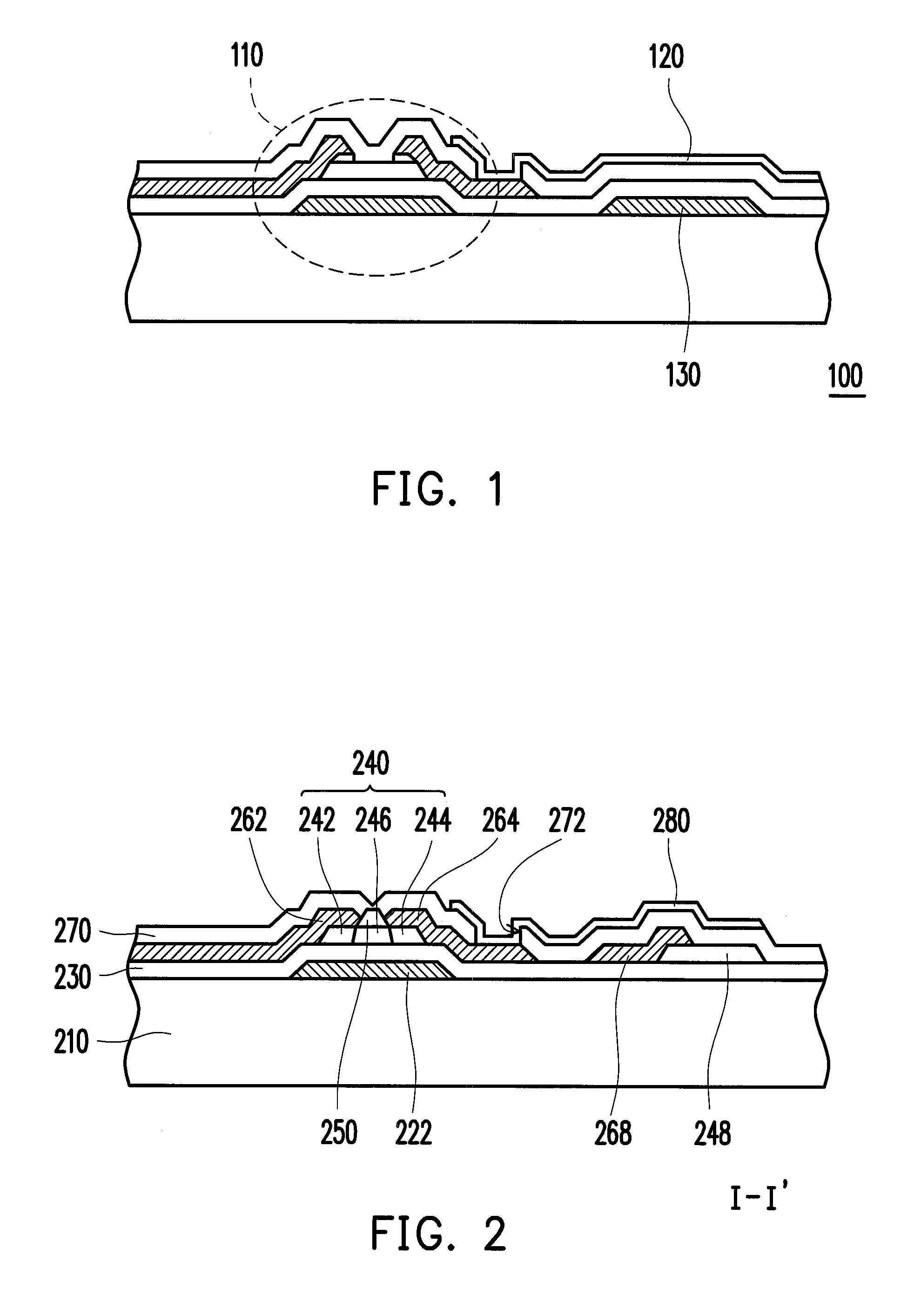
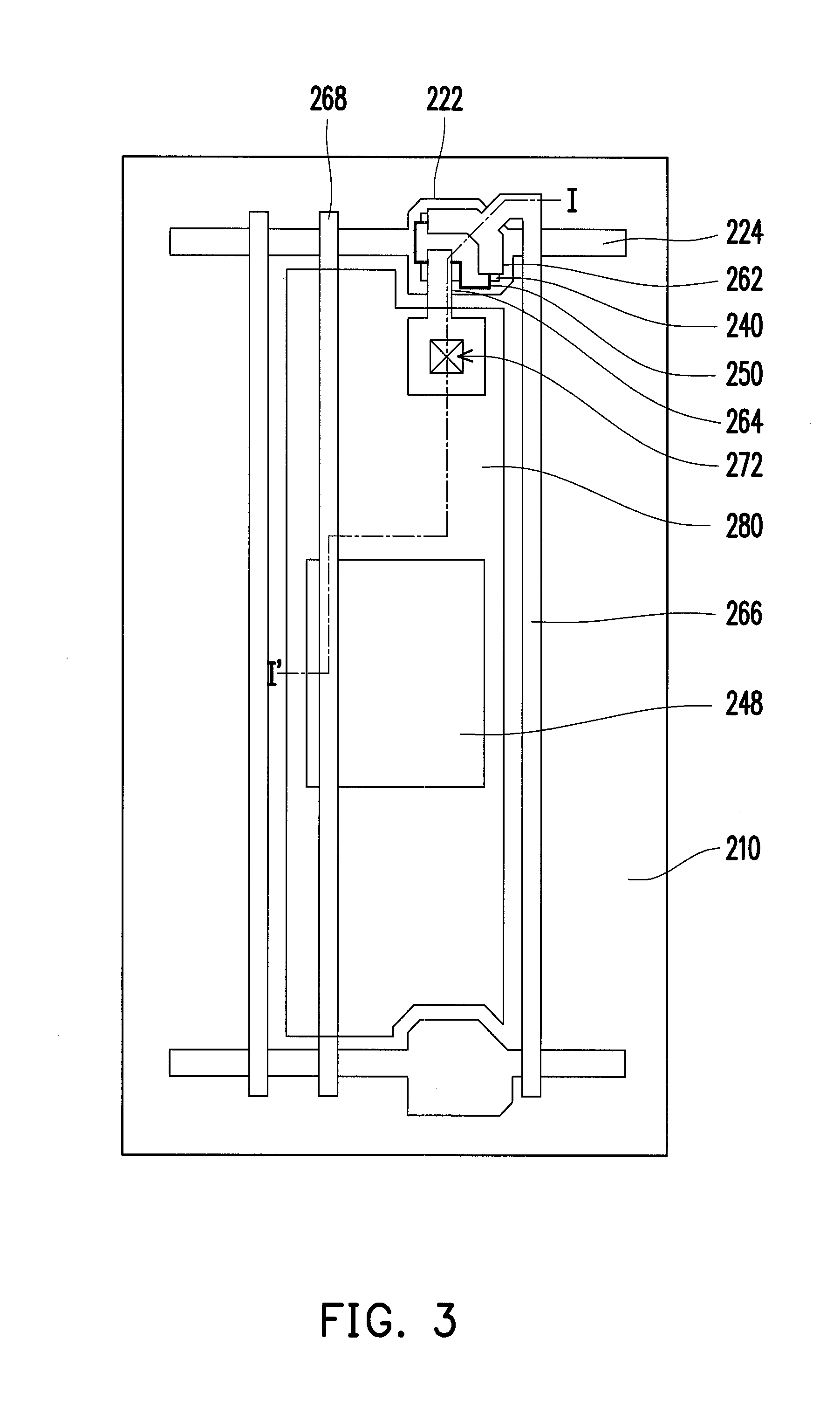
[0033]FIG. 2 illustrates a pixel structure according to an embodiment of the invention. FIG. 3 is a top view illustrating the pixel structure depicted in FIG. 2. As indicated in FIG. 2 and FIG. 3, a gate 222 and a scan line 224 are configured on a substrate 210, and the gate 222 is electrically connected to the scan line 224. In this embodiment, the substrate 210 is exemplarily made of a transparent material, such as glass, plastic, and so on. A gate insulating layer 230 is configured on the substrate 210 and covers the gate 222 and the scan line 224. An active layer 240 is configured on the gate insulating layer 230 and correspondingly located above the gate 222. A material of the active layer 240 is, for instance, an oxide semiconductor material, such as IGZO, InGaZnO, IZO, IGO, ZnO, 2CdO.GeO2, or NiCo2O4, and the active layer 240 includes a source region 242, a drain region 244, and a channel region 246 that have different sheet resistances. The channel region 246 is located betw...


PUM


Abstract

A pixel structure and a manufacturing method thereof are provided. In the pixel structure, an electrode of a storage capacitor is formed when an active layer is formed, and the electrode and the active layer are made of the same material. The material of the electrode and the active layer can be an oxide semiconductor with high transmittance. Therefore, a stable display frame of the pixel structure can be provided by the storage capacitor, an aperture ratio of the pixel structure can be improved, and power consumption can be further reduced.

Description

CROSS-REFERENCE TO RELATED APPLICATION[0001]This application claims the priority benefit of Taiwan application serial no. 99141790, filed Dec. 1, 2010. The entirety of the above-mentioned patent application is hereby incorporated by reference herein and made a part of this specification.BACKGROUND OF THE INVENTION[0002]1. Field of the Invention[0003]The invention relates to a pixel structure and a manufacturing method thereof, and particularly to a pixel structure having a storage capacitor and a manufacturing method of the pixel structure.[0004]2. Description of Related Art[0005]By virtue of the increasing demands for displays and the rising awareness of environmental protection, a thin film transistor liquid crystal display (TFT-LCD) featuring superior properties including high definition, optimal space utilization, low power consumption, and no radiation has gradually become the mainstream product in the market of the displays. To comply with the users' requirements for high cont...

Claims


Application Information

Patent Timeline
Patent Type & Authority Applications(United States)
IPC IPC(8): H01L29/04
CPCG02F1/136213G02F2201/40G02F2202/10H01L29/7869H01L27/1225H01L27/1255H01L29/41733G02F2203/01
Inventor LIN, WU-HSIUNGCHEN, PO-HSUEHCHEN, SHIN-SHUEHSHEN, GUANG-RENYE, JIA-HONG
Owner AU OPTRONICS CORP
Why Eureka
Try Eureka