
Photomasks and methods of manufacturing the same

a technology of photomasks and manufacturing methods, applied in the field of photomasks, can solve the problems of severe deterioration of the quality and reliability of the semiconductor device, the photomask pattern, etc., and achieve the effect of increasing the reliability and economic efficiency of manufacturing semiconductor devices

Active Publication Date: 2012-06-14
SAMSUNG ELECTRONICS CO LTD
View PDF2 Cites 18 Cited by
  • Summary
  • Abstract
  • Description
  • Claims
  • Application Information

AI Technical Summary

Benefits of technology

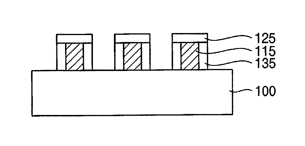
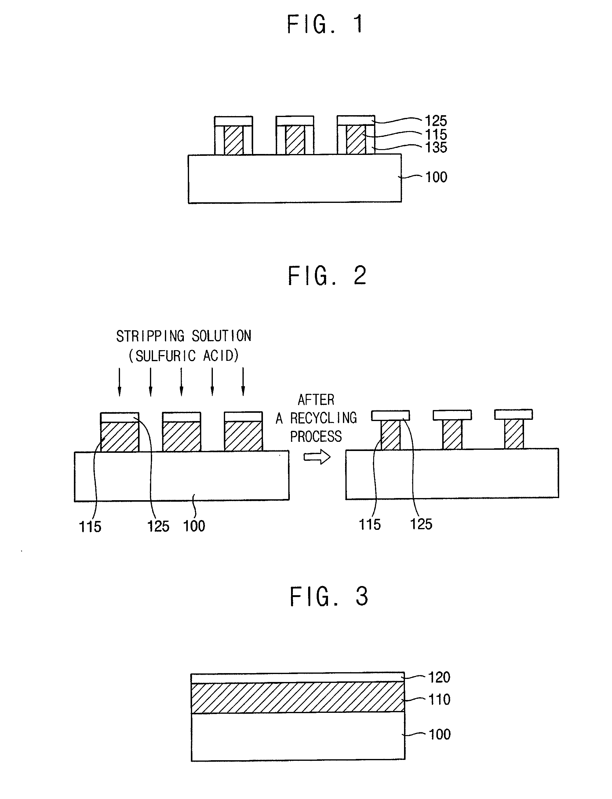
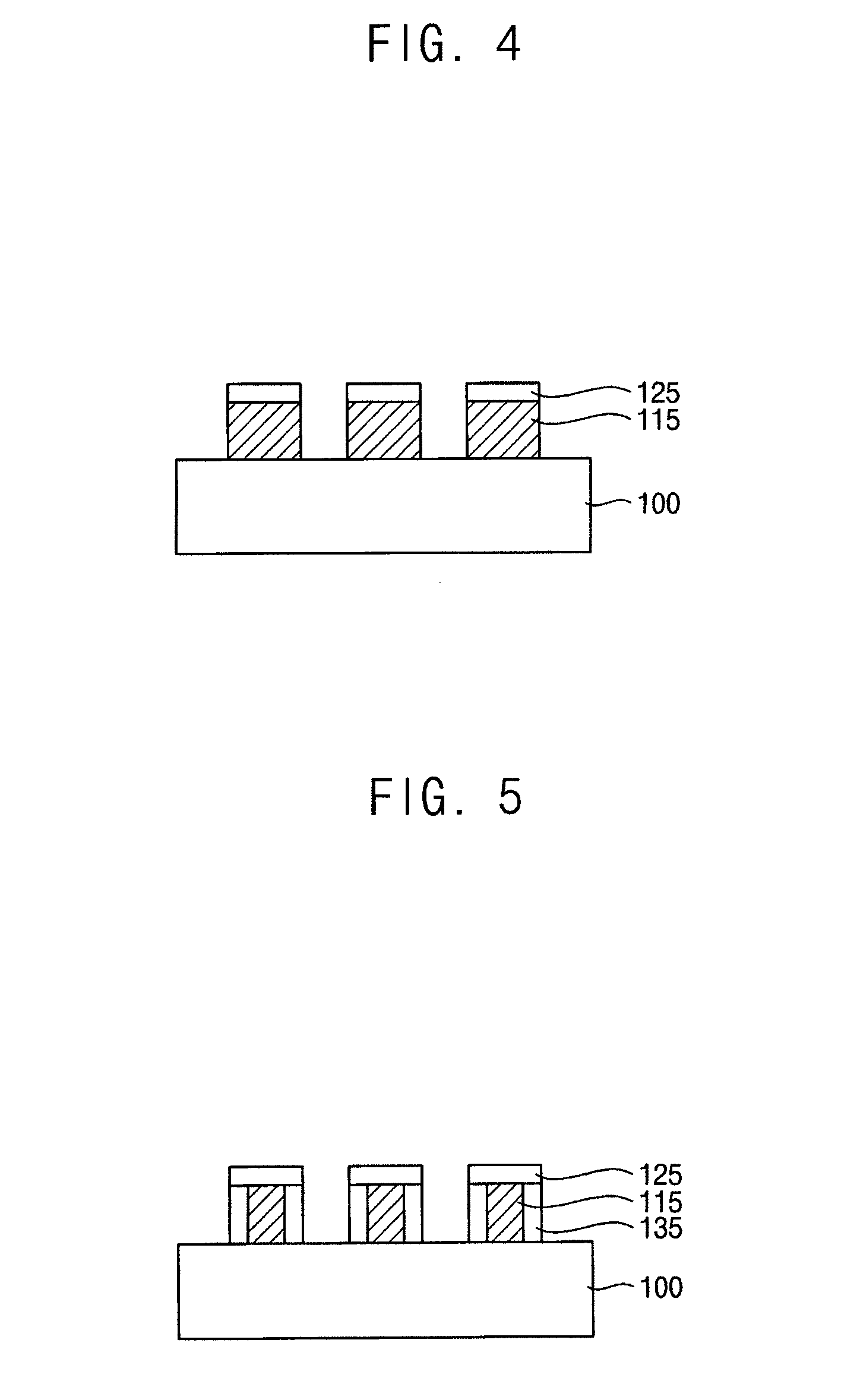
[0025]According to example embodiments, a protection layer pattern including a metal oxide, a metal nitride and/or a metal oxynitride may be formed on a sidewall of a light-shielding layer pattern of a photomask. Thus, the light-shielding layer pattern may be prote

Problems solved by technology

However, an acidic solution used for removing the pellicle may damage the photomask pattern, and a line width of the photomask pattern may be changed.
As semiconductor de

Method used


Image

  • Photomasks and methods of manufacturing the same
  • Photomasks and methods of manufacturing the same
  • Photomasks and methods of manufacturing the same

Examples


Embodiment Construction

[0030]Various example embodiments will be described more fully hereinafter with reference to the accompanying drawings, in which some example embodiments are shown. Example embodiments of the present inventive concept may, however, be embodied in many different forms and should not be construed as limited to example embodiments set forth herein. In the drawings, the sizes and relative sizes of layers and regions may be exaggerated for clarity.

[0031]It will be understood that when an element or layer is referred to as being “on,”“connected to” or “coupled to” another element or layer, it can be directly on, connected or coupled to the other element or layer or intervening elements or layers may be present. Like numerals refer to like elements throughout. As used herein, the term “and / or” includes any and all combinations of one or more of the associated listed items.

[0032]Hereinafter, example embodiments will be explained in detail with reference to the accompanying drawings.

[0033]FI...


PUM


Abstract

In a method of manufacturing a photomask pattern, a light-shielding layer pattern and an anti-reflective layer pattern are formed sequentially on a transparent substrate. Oxidation and nitridation processes are performed on a sidewall of the light-shielding layer pattern to form a protection layer pattern on a lateral portion of the light-shielding layer pattern.

Description

CROSS-REFERENCE TO RELATED APPLICATIONS[0001]This application claims priority under 35 USC §119 to Korean Patent Application No. 10-2010-0126890 filed on Dec. 13, 2010, the disclosure of which is hereby incorporated by reference herein in it's entirety.BACKGROUND[0002]1. Technical Field[0003]Example embodiments relate to photomasks and methods of manufacturing the same. More particularly, example embodiments relate to photomasks including a protection layer pattern and methods of manufacturing the same.[0004]2. Description of the Related Art[0005]A photomask for a photolithography process and an exposure process in manufacturing semiconductor devices may be reused after a recycling process. For example, in the recycling process, a pellicle for protecting the photomask may be removed from the photomask and a pellicle may be re-attached to the photomask by a repellicle process.[0006]However, an acidic solution used for removing the pellicle may damage the photomask pattern, and a line...

Claims


Application Information

Patent Timeline
IPC IPC(8): G03F1/80G03F1/00G03F1/68B82Y30/00
CPCG03F1/68G03F1/80G03F1/54G03F1/46G03F1/48B82Y10/00G03F1/50G03F1/76H01L21/0274H01L21/0337
Inventor OH, JONG-KEUNKANG, DAE-HYUKJEON, CHAN-UKKO, HYUNG-HOHAN, SUNG-JAEKIM, JUNG-JIN
Owner SAMSUNG ELECTRONICS CO LTD
Learn More