Optical semiconductor device and optical module using thereof

a technology of optical modules and semiconductors, applied in semiconductor lasers, optical resonator shapes and constructions, laser details, etc., can solve the problems of limited high-speed interface system throughput and further increase in power consumption, and achieve excellent heat radiation properties, low current operation, and excellent economic efficiency.

Active Publication Date: 2006-12-28
LUMENTUM JAPAN INC
View PDF4 Cites 25 Cited by
  • Summary
  • Abstract
  • Description
  • Claims
  • Application Information

AI Technical Summary

Benefits of technology

[0021] According to the present invention, it is possible to realize the direct modulation laser, having the single lateral mode, in which the chip light power of several milliwatts and the low current operation as a key for the power saving operation are simultaneously realized. In particular, it is possible to realize the 1.3-μm-band light source which is suitable for the short distance application in which the optical fiber trans...

Problems solved by technology

The throughput of these high-speed interface systems is limited by the mounting density depending on the module size and the power consumption in addition to the speed per channel port.
However, in the present circumstance...

Method used


Image

  • Optical semiconductor device and optical module using thereof
  • Optical semiconductor device and optical module using thereof
  • Optical semiconductor device and optical module using thereof

Examples


embodiment 2

[0040]FIG. 8 illustrates a device structure of a 1300-nm-band vertical cavity surface emission type InGaAlAs system short cavity laser according to Embodiment 2 of the present invention. FIG. 8 also illustrates an example of a drive circuit for directly modulating this laser. A basic structure of this laser is basically the same as that of the laser described in Embodiment 1 except for the following points. That is to say, the high reflective film 310 formed in the rear of the laser is replaced with a rear DBR layer 311, the compression strain MQW active layer 302 made of InGaAlAs is left in the rear of the rear DBR layer 311 in order to monitor an output from the device, and an output monitoring electrode 315 is formed at a position corresponding thereto. The device length including the DBR region length is set to the range of 150 to 700 μm similarly to the case of Embodiment 1. In Embodiment 2, in order to emit a laser oscillation beam downward of the substrate 301, a 45°-mirror 3...

embodiment 3

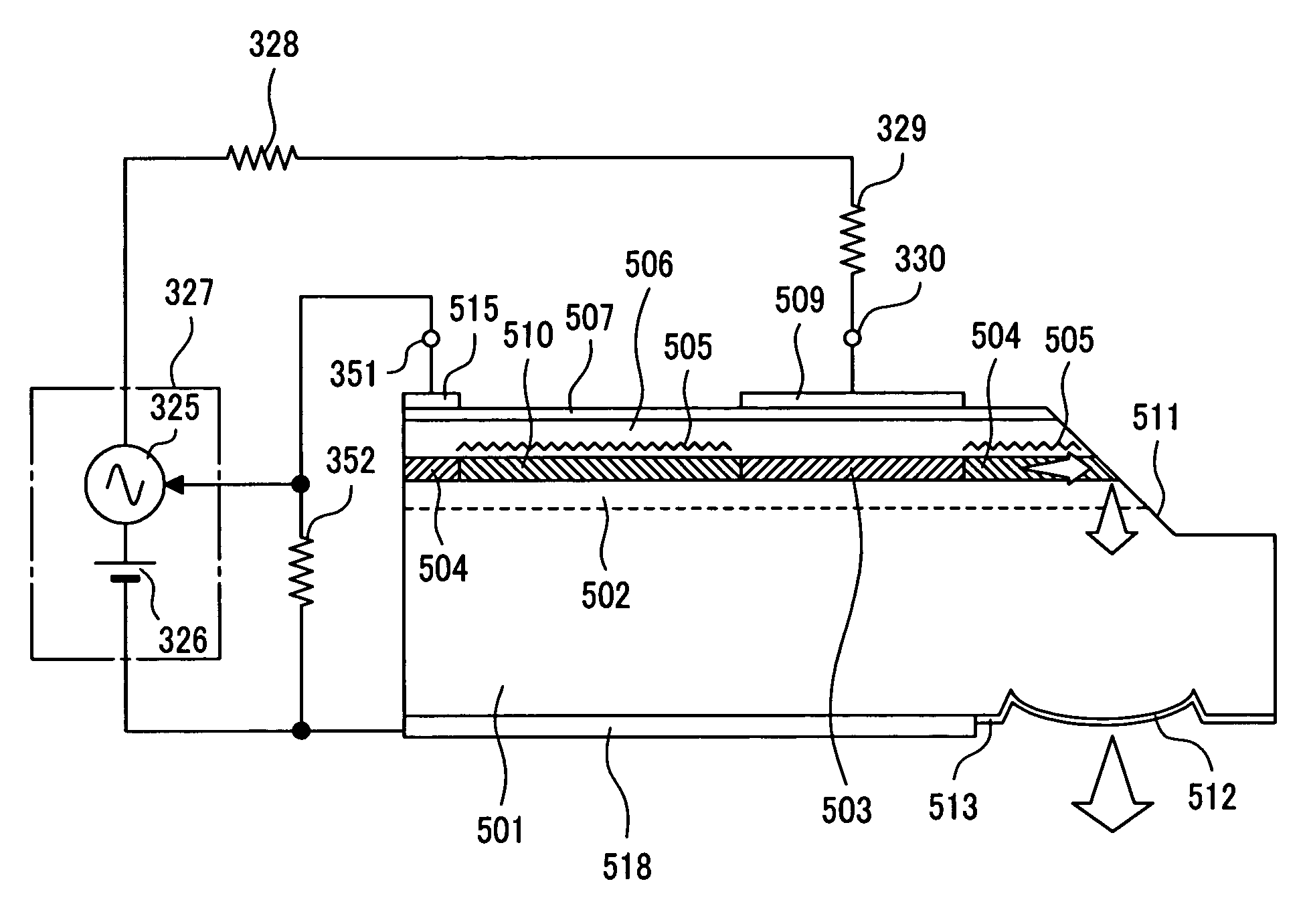
[0045]FIG. 10 is a cross-sectional view of a 1300-nm-band vertical cavity surface emitting laser having a GaInNAs system short cavity DBR structure according to Embodiment 3 of the present invention.

[0046] The laser device is manufactured in accordance with the following procedure. Firstly, an n-type InGaP buffer layer 502, and a GaInNAs-MQW active layer 503 having an emission wavelength of 1300 nm are grown in this order on an n-type GaAs substrate 501 by utilizing a molecular beam epitaxy method. Next, after the GaInNAs-MQW layer 503 has been partially etched away by using an insulator stripe mask, a distributed Bragg reflective (DBR) layer 504 which has a thickness of 300 nm and which is made of bulk GaAs, and a back distributed Bragg reflective (DBR) layer 510 made of GaAs are integrated in a butt-joint form by utilizing the known method. Subsequently, a uniform-pitch grating 505 having a pitch of about 199 nm is formed in a marking manner on the GaAs-DBR layer 504 and the GaAs...

embodiment 4

[0048]FIG. 11 is a cross sectional view of a 1300-nm-band vertical cavity surface emitting laser having a GaInNAs system short cavity distributed feedback (DFB) structure according to Embodiment 4 of the present invention. In the figure, reference numeral 601 designates an n-type GaAs substrate; reference numeral 602 designates an n-type InGaP buffer layer; reference numeral 603 designates a GaInNAs-MQW active layer; reference numeral 604 designates a diffraction grating; reference numeral 604a designates a λ / 4 phase shift structure; reference numeral 605 designates a p-type InGaP cladding layer; reference numeral 606 designates a p+-type GaAs contact layer; reference numeral 608 designates a small electrode pad; reference numeral 609, a GaAs waveguide; reference numeral 610, a 45° C.-mirror; reference numeral 611, a Fresnel lens; reference numeral 612, a non-reflective coating; and 613, an output monitor. At that, a back electrode 618 is provided on the other surface of the n-type ...


PUM


Abstract

The invention aims at realizing a 1300-nm-band direct modulation laser, having a single lateral mode, in which a chip light power of several milliwatts and a low current operation are simultaneously realized. Also, the invention aims at realizing a laser light source excellent in economy as well by realizing output characteristics of a vertical cavity surface light emitting laser. A distributed Bragg reflector laser is constructed in the form of a semiconductor laser having a multilayer structure formed on a predetermined semiconductor substrate. The multilayer structure includes an active region for emitting a laser beam, and a distributed Bragg reflector layer. A length of the active region falls within the range of 10 to 100 μm, and a laser light beam is generated in accordance with ON/OFF of current injection to the active region.

Description

CLAIM OF PRIORITY [0001] The present application claims priority from Japanese application JP 2005-184588 filed on Jun. 24, 2005 the content of which is hereby incorporated by reference into this application. FIELD OF THE INVENTION [0002] The present invention relates to optical semiconductor devices and optical modules using those, and more particularly to optical semiconductor light emitting / receiving devices which are less in electric power and which are suitable for being used in optical communication and the like, and modules using those. BACKGROUND OF THE INVENTION [0003] Along with the abrupt development of the information technology, technology with which large capacity promotion, increase in port mounting density, and economical efficiency of a system are made compatible with one another has become more and more important not only in the conventional communication network (telecom), but also in the datacom such as a storage area network (SAN) or the Ethernet (registered tra...

Claims


Application Information

Patent Timeline
IPC IPC(8): H01S5/00H01S3/08
CPCH01S5/0428H01S5/32391H01S5/125
Inventor AOKI, MASAHIRO
Owner LUMENTUM JAPAN INC
Why Eureka
Try Eureka