Comparator with offset compensation and improved dynamic range
a technology of offset compensation and comparator, applied in the field of comparator, can solve the problems of limiting the accuracy of an adc and limiting the resolution of the comparator
- Summary
- Abstract
- Description
- Claims
- Application Information
AI Technical Summary
Benefits of technology
Problems solved by technology
Method used
Image

Examples
Embodiment Construction
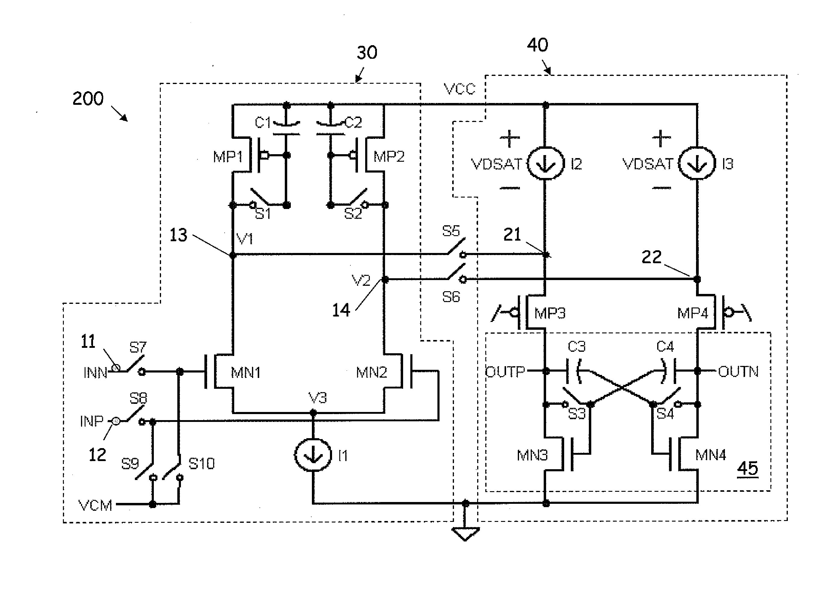
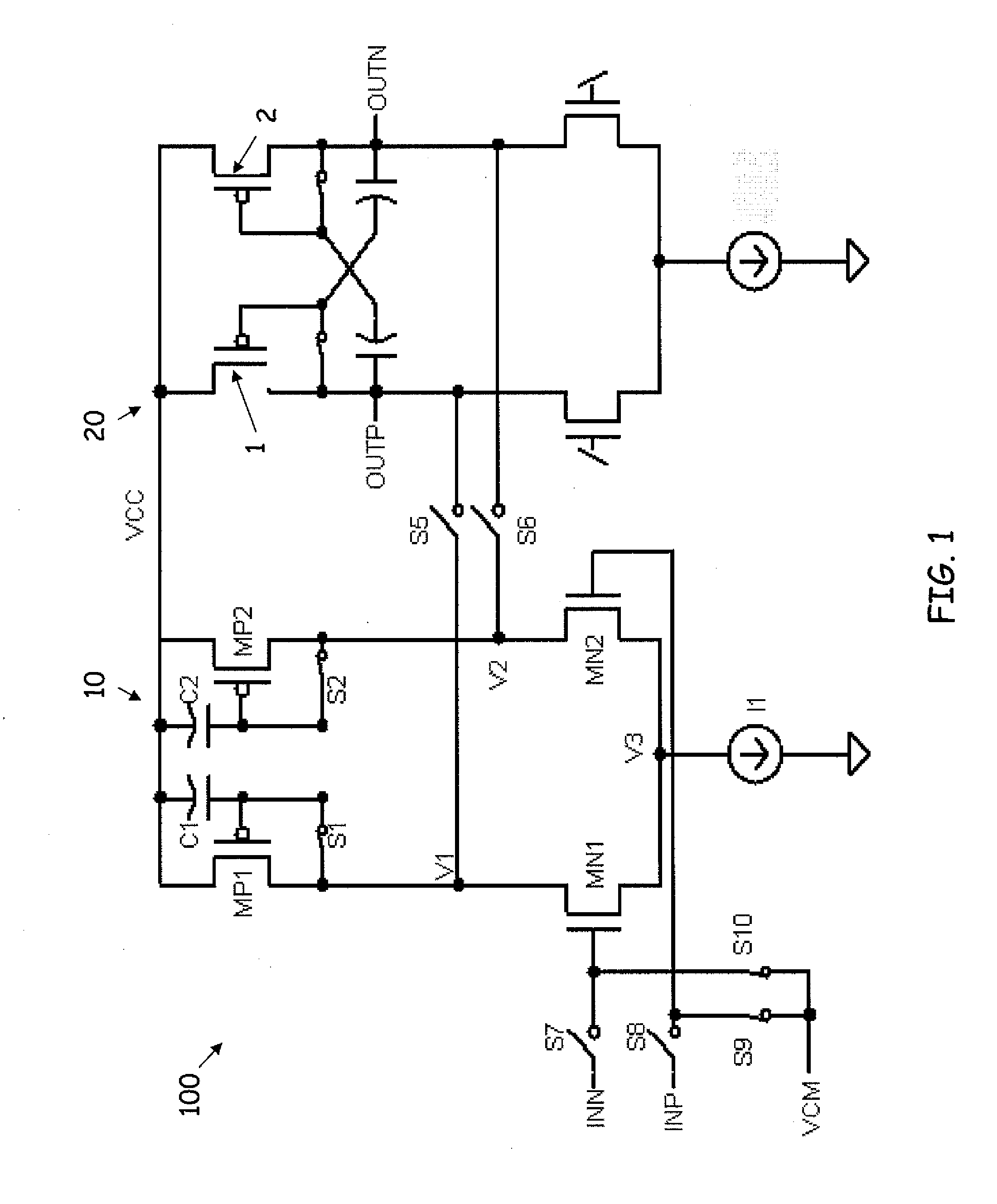
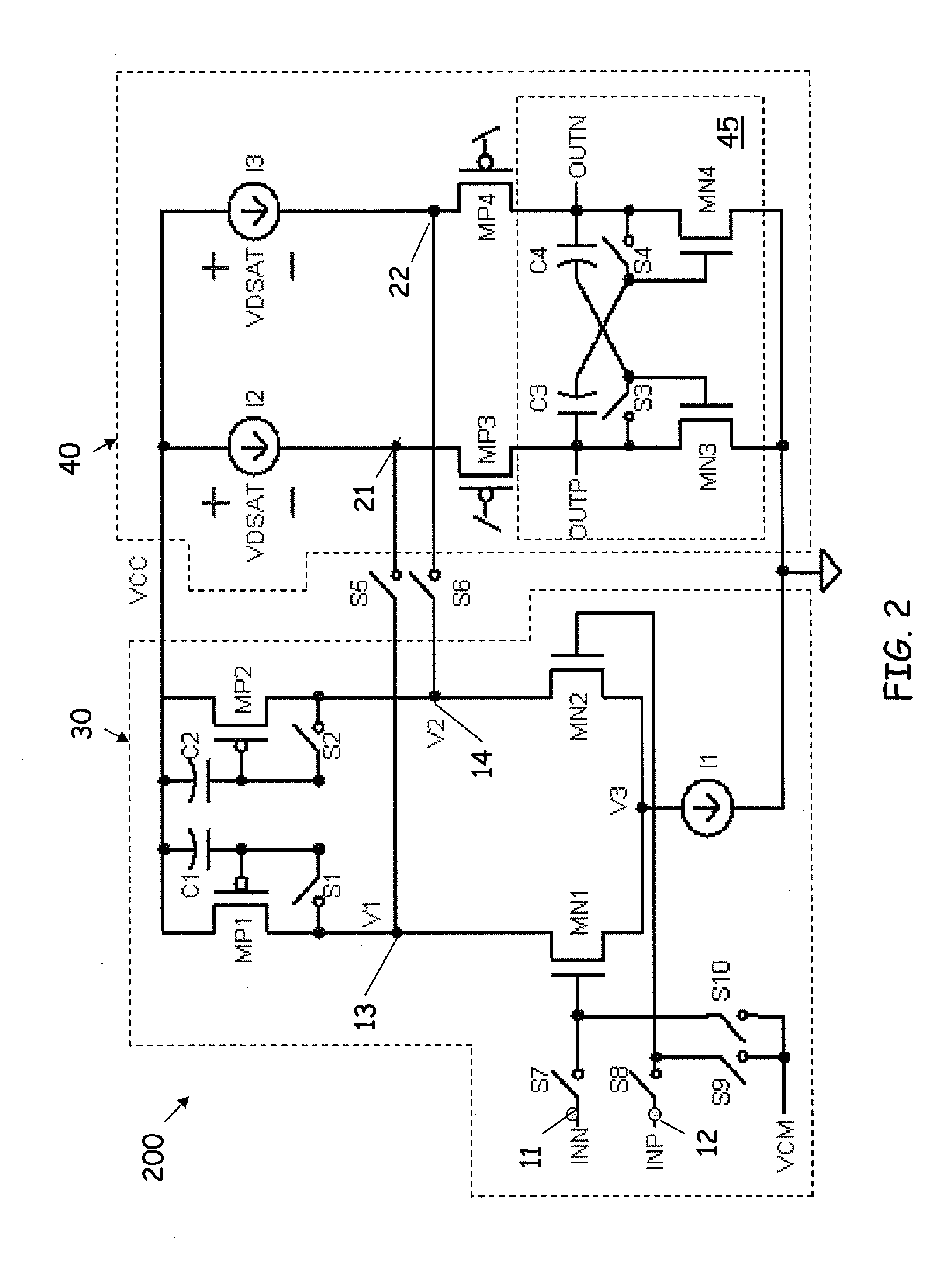
[0019]Although the two-stage comparator architecture of FIG. 1 has various advantages, as described above, it has been appreciated that the comparator 100 may have a limited dynamic range due to the architecture of the second stage 20 of comparator 100. In the circuit of FIG. 1, the voltages V1 and V2 which are provided as inputs to the second stage 20 are limited in value when switches S5 and S6 are turned on because of the voltage drop across the diode-connected PMOS transistors 1 and 2. Voltages V1 and V2 cannot reach a voltage as high as the supply voltage (VCC) because the voltage drop across the diode-connected PMOS transistors 1 and 2 is approximately 0.6 V. For example, if VCC is 1.8 V, the diode drop across PMOS transistors 1 and 2 prevents V1 and V2 from rising above approximately 1.2 V. This constraint on the voltages V1 and V2 limits the allowable range of input voltages INN and INP for comparator 100. When V1 and V2 cannot rise above 1.2 V, the voltage V3 at the common ...
PUM
 Abstract
Description
Claims
Application Information