Solid-state image pickup device and method for driving the same

a solid-state image and pickup device technology, applied in the direction of television systems, envelopes, radio control devices, etc., can solve the problems of disadvantageous sensitivity reduction and decrease in the unit pixel sensitivity, so as to prevent the decrease of sensitivity and increase the frame rate, the amount of each piece of pixel information is doubled, and the effect of increasing the frame ra

Inactive Publication Date: 2005-09-08
SONY CORP
View PDF40 Cites 183 Cited by
  • Summary
  • Abstract
  • Description
  • Claims
  • Application Information

AI Technical Summary

Benefits of technology

[0022] In the solid-state image pickup device having this configuration, analog signals output from the unit pixels are converted to digital values and the digital values are added among a plurality of unit pixels and are read. In terms of the number of pieces of read pixel information, this operation is equivalent to interlaced reading (skip reading) of pixel information. However, the amount of each piece of pixel information is larger by X times if the number of pixels to be added is X. Therefore, even when the exposure time of the unit pixels is reduced to ½ in order to double the frame rate, the amount of each piece of pixel information is doubled by adding digital values of unit pixels between two rows at analog-digital conversion, so that a decrease of sensitivity can be prevented.
[0023] According to the present invention, in the solid-state image pickup device for converting analog signals output from unit pixels through column signal lines to digital values and reading the digital values, the digital values are added among a plurality of unit pixels and the added values are read. With this method, the amount of each piece of pixel information does not decrease even when the exposure time of the unit pixels is reduced. Accordingly, the frame rate can be increased while preventing a decrease in sensitivity.

Problems solved by technology

Therefore, when the frame rate is increased by applying skip reading of pixel information in the CMOS image sensor 100 including column-parallel ADCs, the sensitivity of the unit pixel decreases due to the higher frame rate, and thus the sensitivity of imaging result decreases disadvantageously.

Method used


Image

  • Solid-state image pickup device and method for driving the same
  • Solid-state image pickup device and method for driving the same
  • Solid-state image pickup device and method for driving the same

Examples


first embodiment

(First Embodiment)

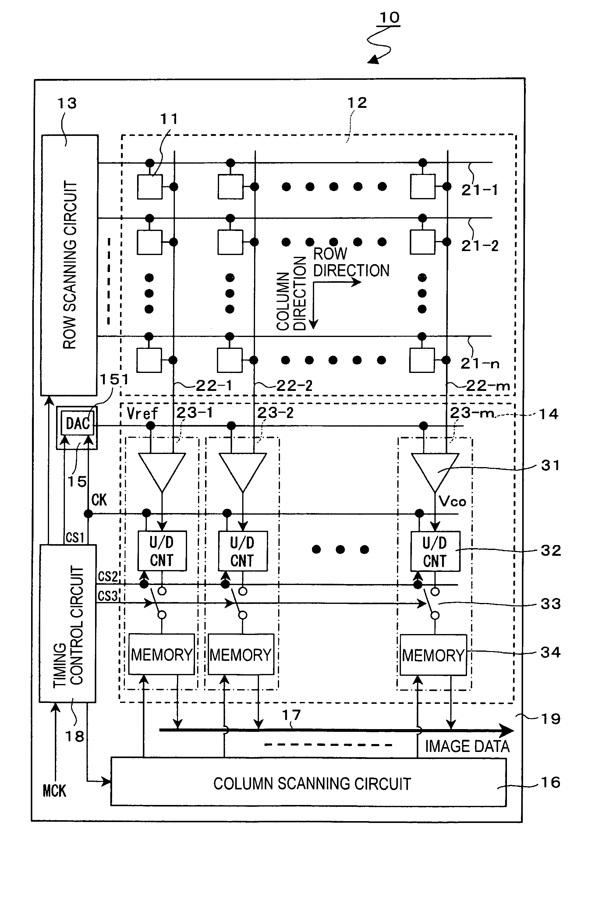
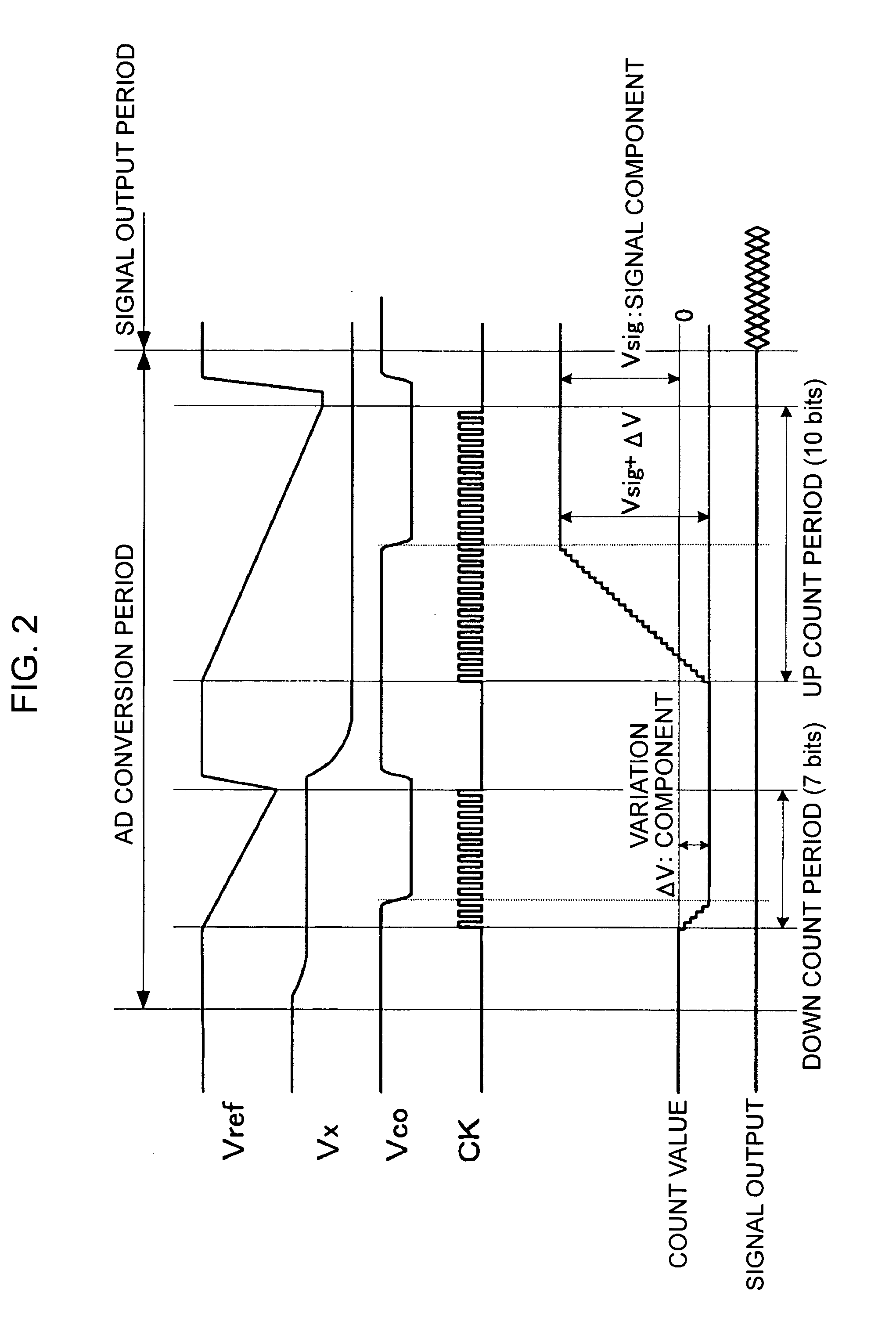
[0043]FIG. 1 is a block diagram showing the configuration of a solid-state image pickup device according to a first embodiment of the present invention, for example, a CMOS image sensor 10 including column-parallel ADCs. As shown in FIG. 1, the CMOS image sensor 10 according to this embodiment includes a pixel array unit 12, where unit pixels 11, each including a photoelectric transducer, are two-dimensionally arranged in a matrix pattern; a row scanning circuit 13, a column processing unit 14; a reference-voltage supplying unit 15; a column scanning circuit 16; a horizontal output line 17; and a timing control circuit 18.

[0044] In this system configuration, the timing control circuit 18 generates clock signals and control signals serving as reference of the operations of the row scanning circuit 13, the column processing unit 14, the reference-voltage supplying unit 15, the column scanning circuit 16, and so on, based on a master clock MCK, and supplies the signa...

second embodiment

(Second Embodiment)

[0090]FIG. 6 is a block diagram showing the configuration of a CMOS image sensor 50 including column-parallel ADCs according to a second embodiment of the present invention. FIG. 7 shows a timing chart for illustrating the operation of the CMOS image sensor 50 according to this embodiment.

[0091] The configuration of the CMOS image sensor 50 including column-parallel ADCs according to this embodiment is basically the same as that of the CMOS image sensor 10 including column-parallel ADCs according to the first embodiment shown in FIG. 1. The difference between them is that a row scanning circuit 13A includes an address decoder capable of selecting arbitrary row control lines 21-i (21-1 to 21-n). The row scanning circuit 13A including the address decoder is capable of sequentially selecting the row control lines 21-1 to 21-n in the order of first row, third row, second row, fourth row, . . . , as shown in FIG. 7, for example.

[0092] In this row scanning, when an ad...

third embodiment

(Third Embodiment)

[0096]FIG. 8 is a block diagram showing the configuration of a CMOS image sensor 60 including column-parallel ADCs according to a third embodiment of the present invention. In FIG. 8, parts which are the same as those in FIG. 1 are denoted by the same reference numerals.

[0097] The configuration of the CMOS image sensor 60 including column-parallel ADCs according to this embodiment is basically the same as that of the CMOS image sensor 10 including column-parallel ADCs according to the first embodiment shown in FIG. 1. The difference between them is as follows.

[0098] The output of each of the ADCs 23-1, 23-3, . . . , connected to the odd-numbered column signal lines 22-1, 22-3, . . . , is output through a horizontal output line 17-1 of an N-bit width. Likewise, the output of each of the ADCs 23-2, 23-4, . . . , connected to the even-numbered column signal lines 22-2, 22-4, . . . , is output through a horizontal output line 17-2 of an N-bit width. The digital signa...


PUM


Abstract

A CMOS image sensor includes column-parallel ADCs. Each of the ADCs includes a comparator and an up/down counter. With this configuration, digital values of pixels in a plurality of rows can be added without using additional circuits, such as an adder and a line memory device, and the frame rate can be increased while maintaining constant sensitivity.

Description

BACKGROUND OF THE INVENTION [0001] 1. Field of the Invention [0002] The present invention relates to a solid-state image pickup device and a method for driving the same. Particularly, the present invention relates to a solid-state image pickup device for converting analog signals output from unit pixels through column signal lines to digital signals and reading the digital signals, and to a method for driving the same. [0003] 2. Description of the Related Art [0004] In recent years, a CMOS image sensor including a column-parallel ADCs (analog-digital converters) has been reported (e.g., see non-Patent Document 1: W. Yang et al., “An Integrated 800×600 CMOS Image System” ISS CC Digest of Technical Papers, pp. 304-305, February 1999). In this CMOS image sensor, ADCs are arranged for respective columns in matrix-patterned unit pixels. [0005]FIG. 15 is a block diagram showing the configuration of a CMOS image sensor 100 including column-parallel ADCs according to a known art. [0006] In ...

Claims


Application Information

Patent Timeline
Patent Type & Authority Applications(United States)
IPC IPC(8): H04N5/335H01L27/146H04N5/341H04N5/347H04N5/374H04N5/376H04N5/378
CPCH03M1/1023H03M1/56H04N5/37455H04N5/347H04N3/1562H04N25/46H04N25/772B42D25/27B42D25/21B42D15/0053B42D25/30B65D27/00H04N25/75H04N23/54H04N25/767
Inventor NITTA, YOSHIKAZUFUKUSHIMA, NORIYUKIMURAMATSU, YOSHINORIYASUI, YUKIHIKO
Owner SONY CORP
Why Eureka
Try Eureka