
Non-volatile semiconductor memory cell with dual functions

Active Publication Date: 2012-06-28
EMEMORY TECH INC
View PDF4 Cites 10 Cited by
  • Summary
  • Abstract
  • Description
  • Claims
  • Application Information

AI Technical Summary

Problems solved by technology

However, the memory cells are slow and inefficient.

Method used


Image

  • Non-volatile semiconductor memory cell with dual functions
  • Non-volatile semiconductor memory cell with dual functions
  • Non-volatile semiconductor memory cell with dual functions

Examples


Embodiment Construction

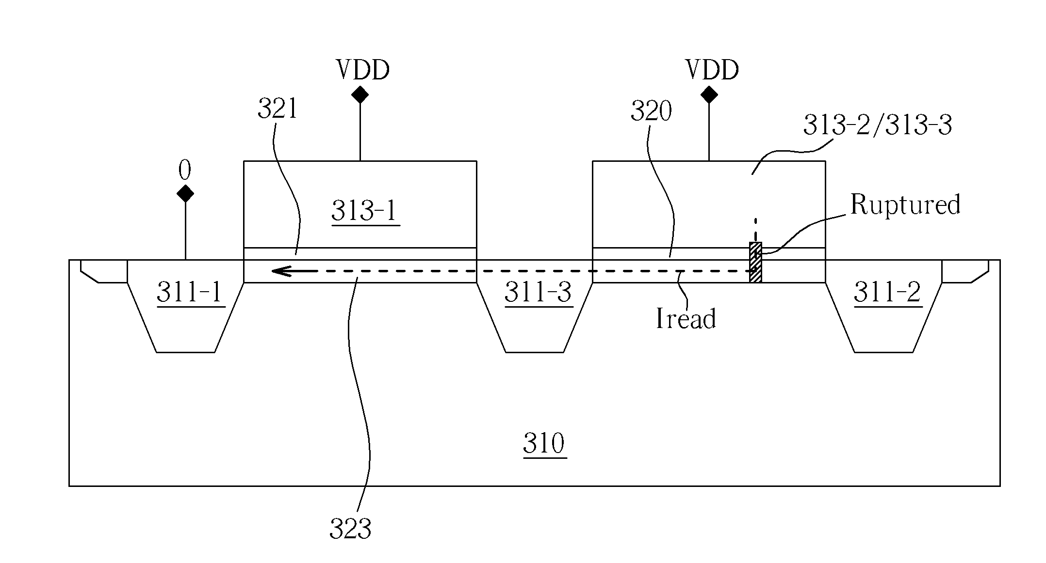
[0023]Please refer to FIG. 3, which is a diagram of a complementary metal-oxide-semiconductor (CMOS) non-volatile memory cell 300 (hereinafter “the memory cell 300”) according to an embodiment of the present invention. The memory cell 300 may be formed over an active region 315 in a P-well region 310 of a substrate. Although CMOS P-well topology is described, the embodiments described herein are also suitable for application to CMOS N-well topology. A first N+ diffusion region 311-1 may be formed on a surface of the active region 315 on a left (second) side of a first polysilicon gate 313-1, a second N+ diffusion region 311-2 may be formed on the surface of the active region 315 on a first side of a second polysilicon gate 313-2 opposite a right (first) side of the first polysilicon gate 313-1, and a third N+ diffusion region 311-3 may be formed on the surface of the active region 315 between the first polysilicon gate 313-1 and the second polysilicon gate 313-2.

[0024]The second pol...


PUM


Abstract

A non-volatile semiconductor memory cell with dual functions includes a substrate, a first gate, a second gate, a third gate, a charge storage layer, a first diffusion region, a second diffusion region, and a third diffusion region. The second gate and the third gate are used for receiving a first voltage corresponding to a one-time programming function of the dual function and a second voltage corresponding to a multi-time programming function of the dual function. The first diffusion region is used for receiving a third voltage corresponding to the one-time programming function and a fourth voltage corresponding to the multi-time programming function. The second diffusion region is used for receiving a fifth voltage corresponding to the multi-time programming function.

Description

CROSS REFERENCE TO RELATED APPLICATIONS[0001]This application claims the benefit of U.S. provisional application No. 61 / 502,336, filed on Jun. 29, 2011 and entitled “Dual functional Non-volatile Semiconductor Memory,” and is a continuation-in-part of U.S. patent application Ser. No. 12 / 633,780, filed on Dec. 8, 2009 and entitled “NON-VOLATILE SEMICONDUCTOR MEMORY DEVICE WITH INTRINSIC CHARGE TRAPPING LAYER,” which claims the benefit of U.S. provisional application No. 61 / 230,099, filed on Jul. 30, 2009 and entitled “Semiconductor Non-volatile Memory.” The disclosures of the prior applications are incorporated herein by reference herein in their entirety.BACKGROUND OF THE INVENTION[0002]1. Field of the Invention[0003]The present invention relates to a non-volatile semiconductor memory cell, and more particularly to a non-volatile semiconductor memory cell with dual functions.[0004]2. Description of the Prior Art[0005]Non-volatile memory is a type of memory that retains information ev...

Claims


Application Information

Patent Timeline
IPC IPC(8): G11C11/34
CPCG11C17/16G11C17/18H01L21/28282H01L29/792H01L27/11568H01L29/42344H01L27/11206H01L29/40117H10B20/20H10B43/30
Inventor LU, HAU-YANCHEN, HSIN-MINGYANG, CHING-SUNG
Owner EMEMORY TECH INC
Learn More