
Leadless semiconductor package with routable leads, and method of manufacture

a technology of leadless semiconductor and leadframe, which is applied in the direction of semiconductor devices, semiconductor/solid-state device details, line/current collector details, etc., can solve the problems of 107/b> not being able to support the bond pad at any significant distance, and unable to be made either wider or thicker

Active Publication Date: 2012-07-05
STMICROELECTRONICS SRL
View PDF5 Cites 7 Cited by
  • Summary
  • Abstract
  • Description
  • Claims
  • Application Information

AI Technical Summary

Problems solved by technology

There are two conflicting problems that affect the reliability of this device.
This arrangement is likely prone to shorting between the wires during the encapsulation process because of their excessive length and close proximity. this problem could be reduced somewhat if the bond pads were moved closer to the center of the device so the wires could be shortened, but this raises a different problem.
Given their small dimensions, the leads 107 are not capable of supporting bond pads at any significant distance.
On the other hand, they cannot be made either wider or thicker without risking contact with other leads or with underlying circuit board pads.
This arrangement is again unreliable, and prone to shorting during handling steps prior to encapsulation.
A problem that arises here is that, when the flip chip die 302 is positioned on the fingers 304 by a place-and-pick machine, they have a tendency to flex slightly, then spring back when the machine releases, causing the die 302 to bounce, sometimes bouncing enough to shift the die out of alignment with the fingers 30

Method used


Image

  • Leadless semiconductor package with routable leads, and method of manufacture
  • Leadless semiconductor package with routable leads, and method of manufacture
  • Leadless semiconductor package with routable leads, and method of manufacture

Examples


Embodiment Construction

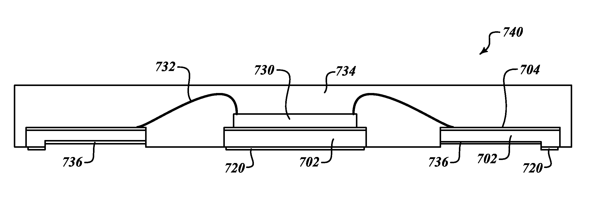
[0019]The problems encountered by the prior art devices described above are eof concern primarily because of the increase in density of contacts, and the need to span greater distances laterally between contact pads of a semiconductor substrate and the corresponding contact pad of the package. Bond wires cannot safely exceed some maximum length, so it is necessary to move the bond pads to which the wires are coupled closer to the center of the package. This in turn requires that leadframe leads be increased in length. At the same time, as the ends of the leads are brought closer to the center, they must be made narrower to fit in the smaller area. Finally, it must be born in mind that bottom surfaces of elements of the leadframe will be exposed at the bottom of the semiconductor package after encapsulation. Where a lead extends across the back side of a package, it creates the potential for short circuits between elements of a circuit board. Because flat “no-lead” packages are mount...


PUM

PropertyMeasurementUnit
aspect ratioaaaaaaaaaa
thickness T1aaaaaaaaaa

Abstract

A leadless semiconductor package includes a package body on a leadframe that includes a die paddle and a plurality of high-aspect-ratio leads, each coupled at a first end to a contact pad of the package, and at a second end to a semiconductor die mounted to the die paddle. During manufacture of the package, molding compound is deposited over a face of the leadframe on which the die paddle and leads are positioned. After the molding compound is cured, a back side of the leadframe is etched to isolate the die paddle and leads, and to thin a portion of each of the leads. Back surfaces of the leads remain exposed at a back face of the body. The thinned portions of the leads are covered with a dielectric. During manufacture of the leadframe, a parent substrate is etched to define the die paddle and a plurality of leads on one side of the substrate and a plurality of cavities on the opposite face.

Description

BACKGROUND OF THE INVENTION[0001]1. Technical Field[0002]The present disclosure relates to semiconductor packaging, and in particular to leadframe-based packages, to leadframes employed in such packages, and most particularly to flat, leadless type packages and leadframes, such as, e.g., QFN packages.[0003]2. Description of the Related Art[0004]While significant advances have been made in semiconductor packaging, including the development of a very large number of packaging types, the majority of semiconductor devices still employ leadframe based packages. This is due to a number of reasons. In particular, leadframe packages are relatively inexpensive to produce, are well known and understood, the tooling is already in hand or readily available, etc. Additionally, leadframe packages have some advantages over many other packages, including having better thermal transmission characteristics, and more being more robust. As industry demand moves toward smaller packages and higher contac...

Claims


Application Information

Patent Timeline
Patent Type & Authority Applications(United States)
IPC IPC(8): H01L23/495H01L21/64H01L21/60
CPCH01L21/4828H01L2924/00014H01L23/3107H01L23/49548H01L23/49582H01L24/13H01L24/16H01L24/48H01L24/49H01L2224/131H01L2224/16245H01L2224/48091H01L2224/48247H01L2224/49171H01L2224/49433Y10T29/49121H01L21/4832H01L2224/45099H01L2924/00H01L2924/014H01L2924/14H01L2924/181H01L2924/00012H01L2224/45015H01L2924/207
Inventor TAN, JERRYCABREROS, WILLIAM
Owner STMICROELECTRONICS SRL
Learn More