Read methods of semiconductor memory device

Inactive Publication Date: 2012-07-05
SK HYNIX INC
View PDF1 Cites 16 Cited by
  • Summary
  • Abstract
  • Description
  • Claims
  • Application Information

AI Technical Summary

Benefits of technology

[0010]According to exemplary embodiments, when the read operation of target cells is performed, the read voltage of the target cells is changed depending on a result of the read operatio

Problems solved by technology

Here, when additional cells are programmed after target cells are programmed in a program operation, the threshold voltages of previousl

Method used


Image

  • Read methods of semiconductor memory device
  • Read methods of semiconductor memory device
  • Read methods of semiconductor memory device

Examples


first embodiment

[0036]FIG. 4 is a flowchart illustrating a read method according to this disclosure.

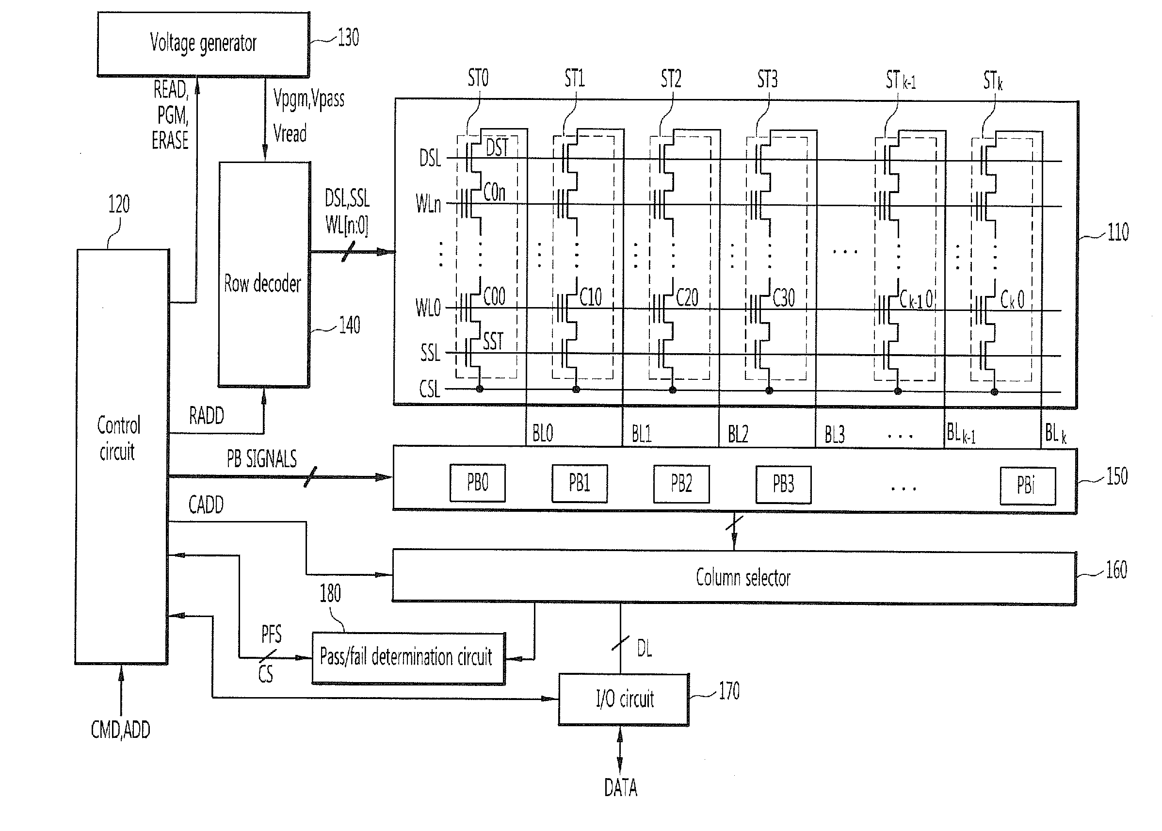
[0037]Referring to FIG. 4, the threshold voltages of memory cells may be classified into an erase state, a first program state, a second program state, and a third program state. The erase state refers to a state in which the threshold voltage is lower than a ground voltage 0 V, the first program state refers to a state in which the threshold voltage has the lowest level (e.g., non-erase-state voltage level), and the third program state refers to a state in which the threshold voltage has the highest level. In the following embodiments, three program states are described as an example, but the threshold voltage may have three or more program states. The read operation of the first embodiment is performed as follows.

[0038](Step 401) Read Data of Target Cells

[0039]When the read operation is started, the data of target cells to be read is read by using a start read voltage Vread=R0. If memory cells coup...

second embodiment

[0054]FIG. 5 is a flowchart illustrating a read method according to this disclosure.

[0055](Step 501) Read Data of Target Cells

[0056]When the read operation is started, the data of target cells to be read is read. In the read operation, a start read voltage Vread is R0.

[0057](Step 502) Check ECC

[0058]It is determined whether an error correction operation is feasible based on the read data of the target cells and an error correction code. If, as a result of the determination, the error correction operation is determined to be feasible, the read operation of the target cells is finished.

[0059](Step 503) Read Data of Adjacent Cells

[0060]If, as a result of the determination at step 502, the error correction operation is determined to be unfeasible, the data of adjacent cells adjacent to the target cells is read. Here, the adjacent cells are coupled to the same word line as the target cells, but belong to different cell strings from the cell strings of the target cells.

[0061](Step 504) De...

third embodiment

[0086]FIG. 6 is a flowchart illustrating a read method according to this disclosure.

[0087](Step 601) Read Data of Target Cells

[0088]When the read operation is started, the data of target cells to be read is read. In the read operation, a start read voltage Vread is R0.

[0089](Step 602) Check ECC

[0090]It is determined whether an error correction operation is feasible based on the read data of the target cells and an error correction code. If, as a result of the determination, the error correction operation is determined to be feasible, the read operation of the target cells is finished.

[0091](Step 603) Read data of adjacent cells

[0092]If, as a result of the determination at step 602, the error correction operation is determined to be unfeasible, the data of two adjacent cells belonging to the same string as the target cells, from among adjacent cells adjacent to the target cells, is read.

[0093](Step 604) Determine states of adjacent cells

[0094]The states of the adjacent cells are dete...


PUM


Abstract

A read method of a semiconductor memory device includes performing a read operation on target cells by using a first read voltage, terminating the read operation on the target cells if, as a result of the read operation on the target cells, error correction is feasible, performing a read operation on first cells next to the target cells along a first direction if, as a result of the read operation on the target cells, error correction is unfeasible, performing the read operation again on the target cells by selecting one of a plurality of read voltages in response to a result of the read operation on the first cells and by using the selected read voltage for reading data of the target cells, and terminating the read operation on the target cells if error correction is feasible.

Description

CROSS-REFERENCE TO RELATED APPLICATION[0001]Priority to Korean patent application number 10-2011-0000113 filed on Jan. 3, 2011, the entire disclosure of which is incorporated by reference herein, is claimed.BACKGROUND[0002]Exemplary embodiments relate to read methods of a semiconductor memory device and, more particularly, to read methods of a non-volatile memory device.[0003]FIG. 1 is a circuit diagram of a memory cell array for illustrating a conventional read method.[0004]Referring to FIG. 1, a semiconductor memory device includes a memory cell array for storing data. The memory cell array includes a plurality of memory cell blocks. For illustration purposes, one of the plurality of memory cell blocks is shown in FIG. 1. The memory cell block is described in detail below.[0005]The memory cell block includes a plurality of cell strings ST0 to STk. Each (for example, ST0) of the cell strings includes a drain select transistor DST coupled to a bit line BL0, a source select transisto...

Claims


Application Information

Patent Timeline
IPC IPC(8): G11C16/26G11C16/04
CPCG11C11/5642G11C16/26G11C16/0483G11C16/34G11C29/00
Inventor ARITOME, SEIICHISEO, SOON OK
Owner SK HYNIX INC
Why Eureka
Try Eureka