Light emitting diode package

a technology of led chips and led chips, applied in the direction of basic electric elements, electrical equipment, semiconductor devices, etc., can solve the problem of uneven distribution of light emitted from led chips

Inactive Publication Date: 2012-07-12
ADVANCED OPTOELECTRONICS TECH
View PDF5 Cites 2 Cited by
  • Summary
  • Abstract
  • Description
  • Claims
  • Application Information

AI Technical Summary

Problems solved by technology

Moreover, distribution of light e...

Method used


Image

  • Light emitting diode package
  • Light emitting diode package
  • Light emitting diode package

Examples


Embodiment Construction

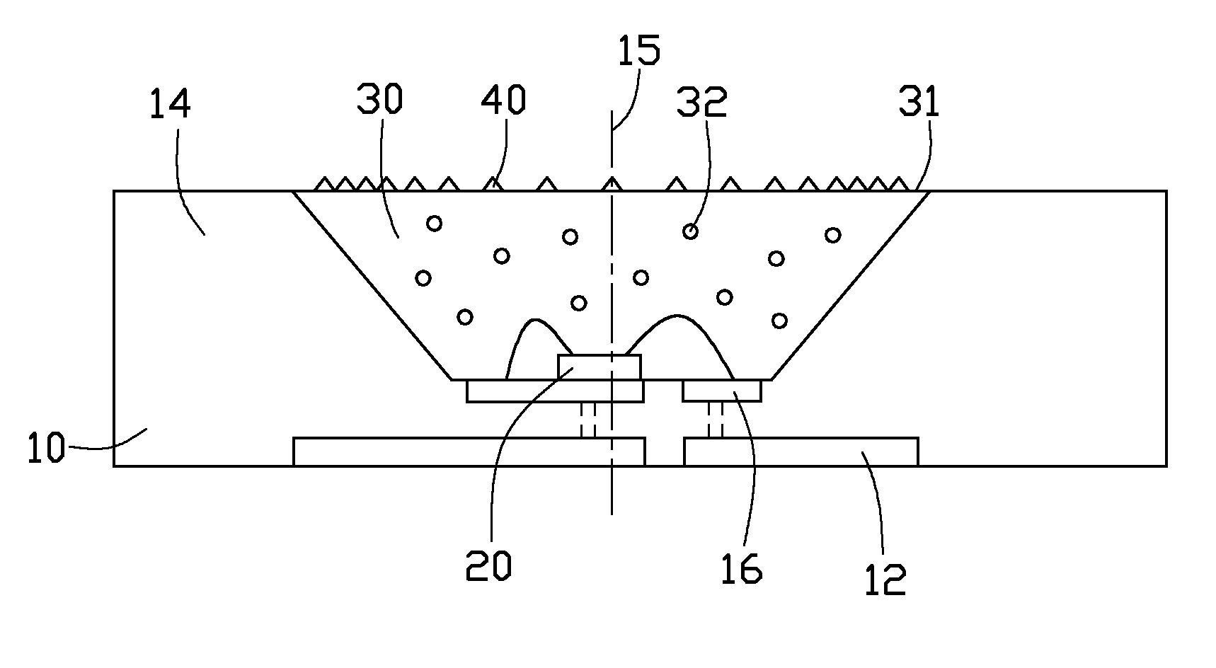
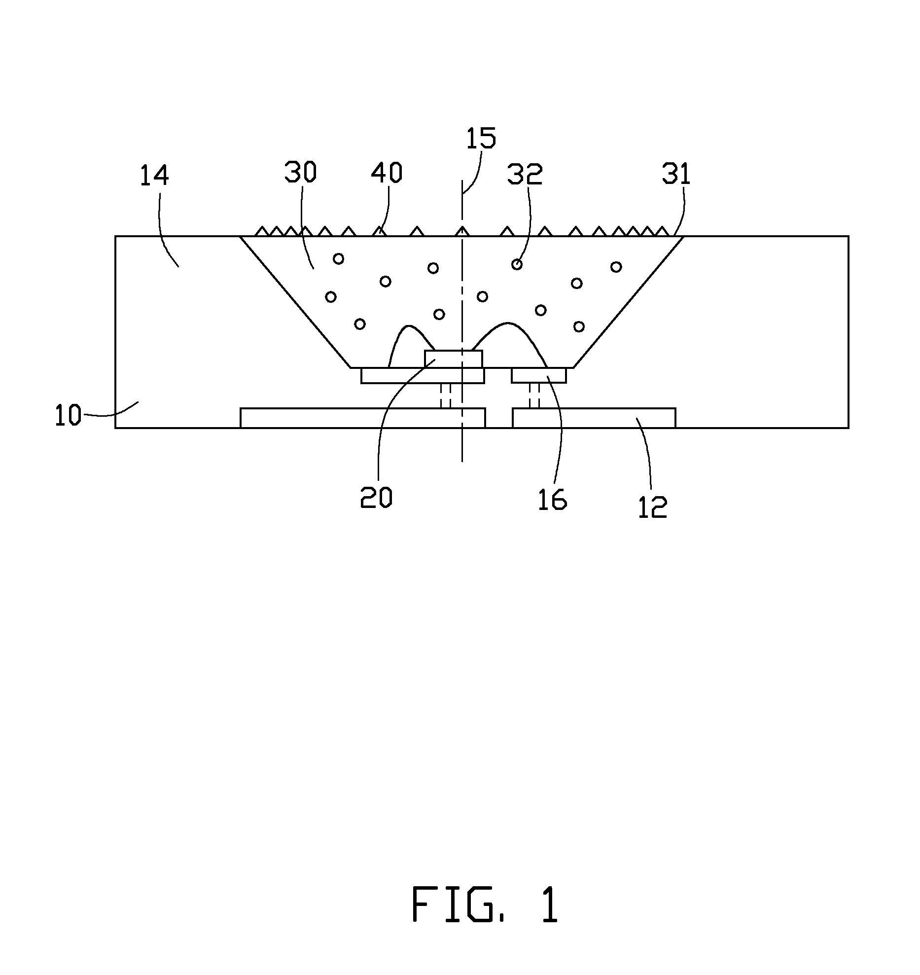
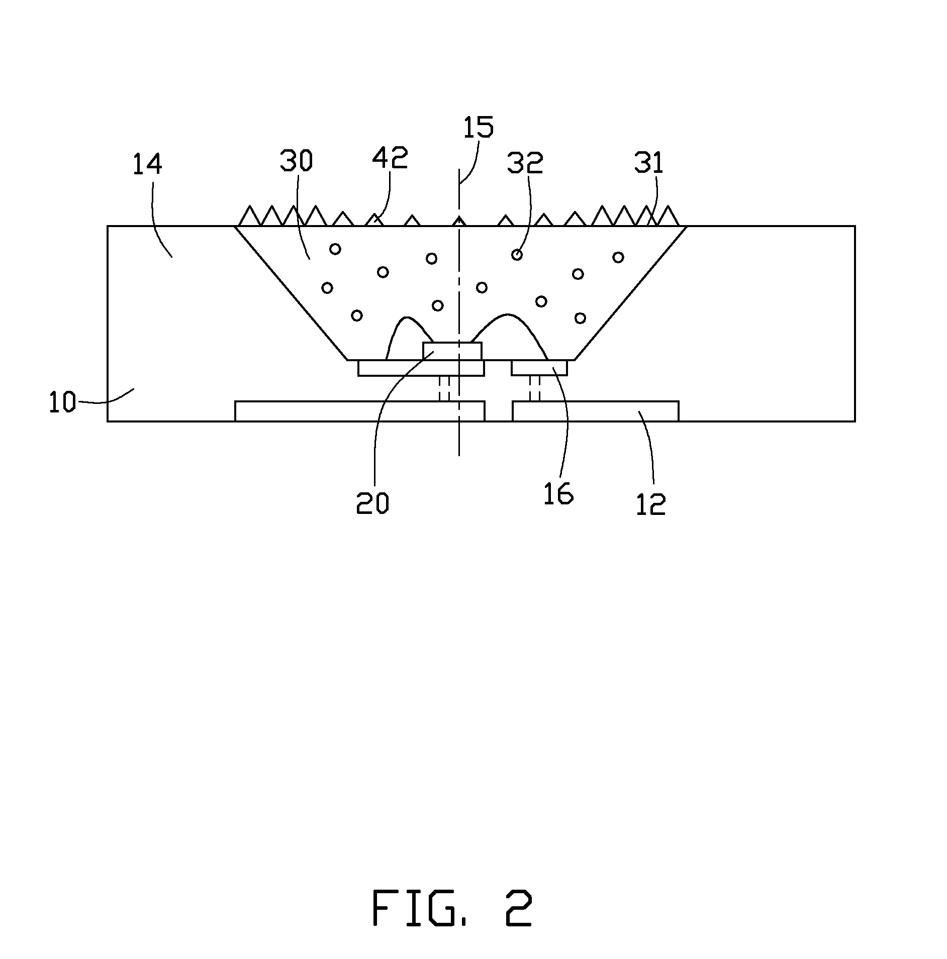
[0008]Referring to FIG. 1, wherein a first embodiment of an LED package in accordance with the present disclosure is shown. The LED package includes a substrate 10, an LED chip 20 attached to the substrate 10, a reflective cup 14 encircling the LED chip 20, and an encapsulant layer 30 filled in the reflective cup 14 and encapsulating the LED chip 20.

[0009]In the embodiment shown in FIG. 1, the substrate 10 is a flat plate. A circuit structure is formed on the substrate 10. The circuit structure includes two internal electrodes 16 formed on a top face of the substrate 10, and two external electrodes 12 formed on a bottom face of the substrate 10. Each of the two internal electrodes 16 is electrically connected to each of the two external electrodes 12.

[0010]The LED chip 20 is disposed on one of the two internal electrodes 12, and electrically connected to each of the two internal electrodes 12 by a lead wire. The LED chip 20 has an optical axis 15 perpendicular to the substrate 10. T...


PUM


Abstract

A light emitting diode package includes a base, a chip mounted on the base, and an encapsulant layer encapsulating the chip. The encapsulant layer includes a light exit face for light generated generated by the chip transmitting through. A plurality of microstructures are formed on the light exit face. Distribution of the microstructures has the following characters: a density of the microstructures is inversely proportional to a light intensity of the light at the light exit face; and a size of the microstructures is inversely proportional to the light intensity of the light at the light exit face.

Description

BACKGROUND[0001]1. Technical Field[0002]The present disclosure generally relates to a light emitting diode (LED) package.[0003]2. Description of Related Art[0004]Light emitting diodes (LEDs) as a new type of light source may generate brighter light than conventional light sources, and may have many advantages, such as energy saving, environment friendliness, and a long life-span. The LED generally includes an LED chip and a transparent encapsulant layer encapsulating the LED chip. Since a refractive index of the encapsulant layer is larger than that of the air, when an incidence angle of incident light of the LED chip is larger than a critical angle, total reflection of the incident light will occur at an interface between the encapsulant layer and the air, under which condition light cannot radiate out of the encapsulant layer. Moreover, distribution of light emitted from the LED chip may be uneven. A larger angle between the incident light and a central axis of the LED chip will r...

Claims


Application Information

Patent Timeline
IPC IPC(8): H01L33/60
CPCH01L2933/0091H01L33/54H01L2224/48091H01L2224/48227H01L2924/00014
Inventor FANG, JUNG-HSIHSU, SHIH-YUAN
Owner ADVANCED OPTOELECTRONICS TECH
Why Eureka
Try Eureka