Hybrid contact structure with low aspect ratio contacts in a semiconductor device

Active Publication Date: 2012-07-19
GLOBALFOUNDRIES US INC
View PDF9 Cites 14 Cited by
  • Summary
  • Abstract
  • Description
  • Claims
  • Application Information

AI Technical Summary

Benefits of technology

[0016]Generally, the present disclosure provides semiconductor devices and manufacturing techniques in which a hybrid contact element may be provided in order to significantly increase the overall conductivity of the contact elements for a given device geometry, while at the same time a significant portion of the contact element may comprise a conductive material of superior conductivity, thereby also increasing the overall conductivity of the contact elements. To this end, any appropriate and well-established contact regime may be appl

Problems solved by technology

Due to the large number of circuit elements and the required complex layout of modern integrated circuits, the electrical connections of the individual circuit elements may generally not be established within the same level on which the circuit elements are manufactured, but require one or more additional wiring layers, which are also referred to as metallization layers.
Despite these advantages, copper also exhibits a number of disadvantages regarding the processing and handling of copper in a semiconductor facility.
For instance, copper readily diffuses in a plurality of well-established dielectric materials, such as silicon dioxide, wherein even minute amounts of copper, accumulating at sensitive device regions, such as contact regions of transistor elements, may lead to a failure of the respective device.
For this reason, great efforts have to be made so as to reduce or avoid any

Method used


Image

  • Hybrid contact structure with low aspect ratio contacts in a semiconductor device
  • Hybrid contact structure with low aspect ratio contacts in a semiconductor device
  • Hybrid contact structure with low aspect ratio contacts in a semiconductor device

Examples


Example

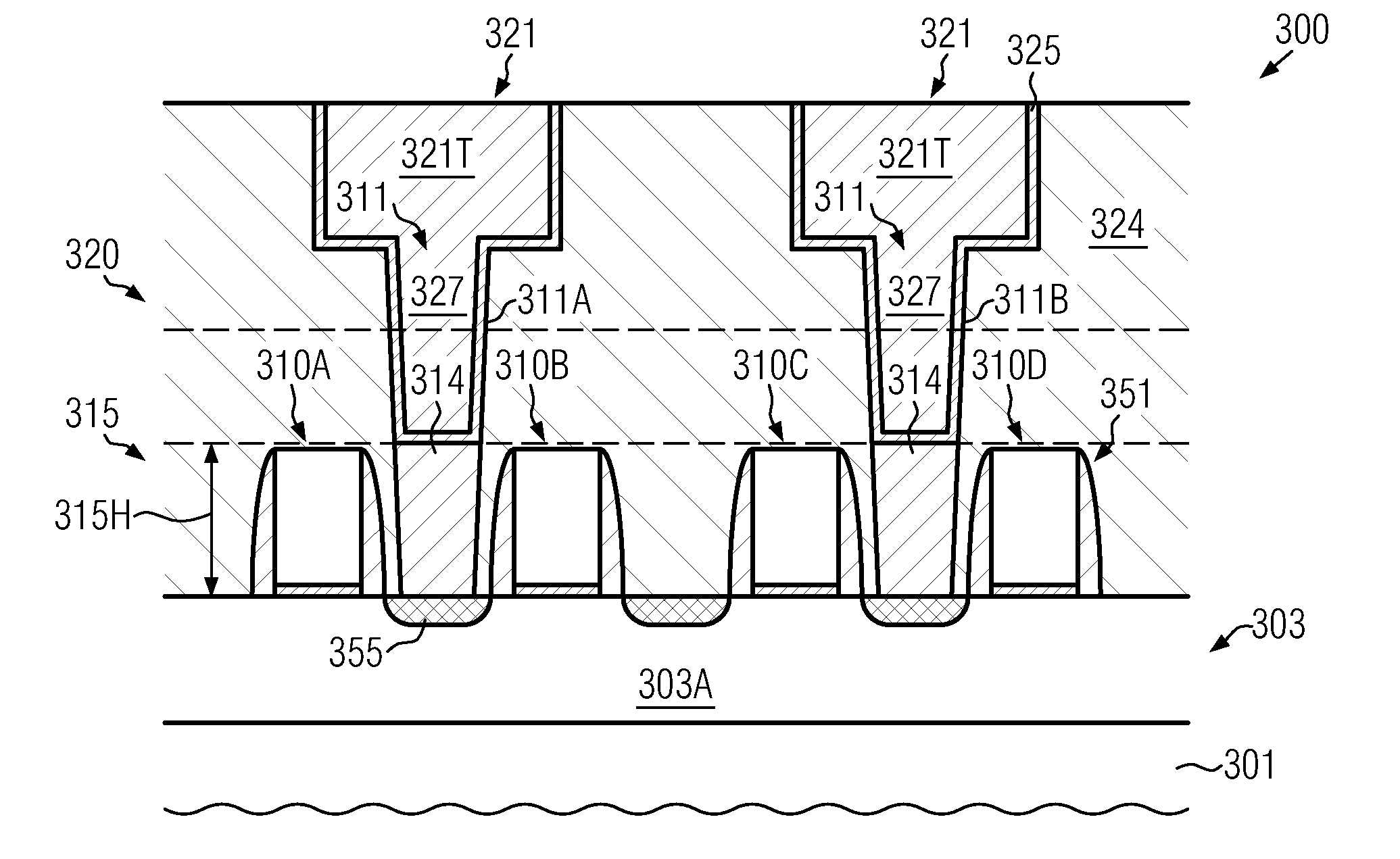
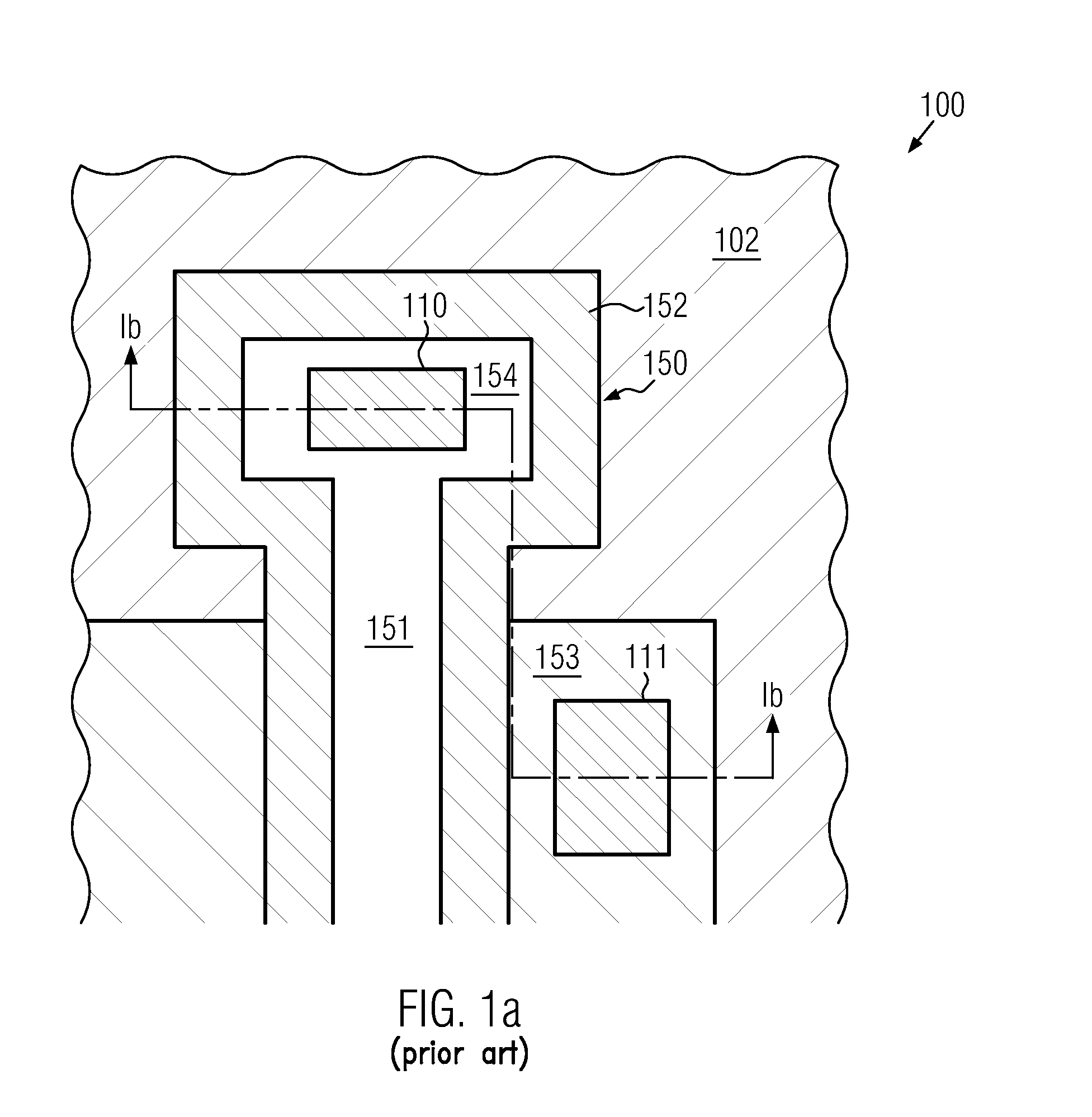
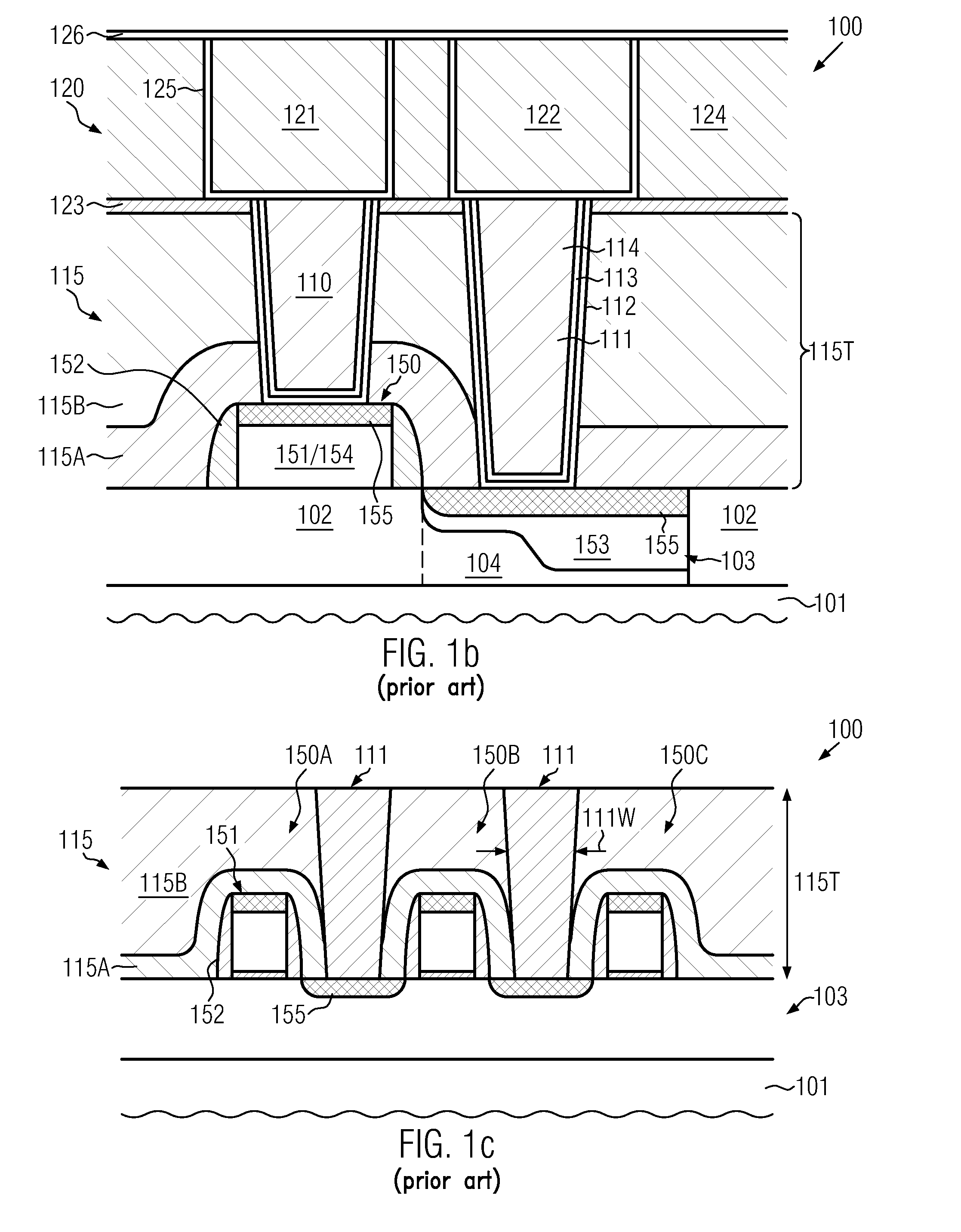
[0026]While the subject matter disclosed herein is susceptible to various modifications and alternative forms, specific embodiments thereof have been shown by way of example in the drawings and are herein described in detail. It should be understood, however, that the description herein of specific embodiments is not intended to limit the invention to the particular forms disclosed, but on the contrary, the intention is to cover all modifications, equivalents, and alternatives falling within the spirit and scope of the invention as defined by the appended claims.

DETAILED DESCRIPTION

[0027]Various illustrative embodiments of the invention are described below. In the interest of clarity, not all features of an actual implementation are described in this specification. It will of course be appreciated that in the development of any such actual embodiment, numerous implementation-specific decisions must be made to achieve the developers' specific goals, such as compliance with system-rel...


PUM


Abstract

In sophisticated semiconductor devices, superior contact resistivity may be accomplished for a given contact configuration by providing hybrid contact elements, at least a portion of which may be comprised of a highly conductive material, such as copper. To this end, a well-established contact material, such as tungsten, may be used as buffer material in order to preserve integrity of sensitive device areas upon depositing the highly conductive metal.

Description

BACKGROUND OF THE INVENTION[0001]1. Field of the Invention[0002]The present disclosure generally relates to the field of semiconductor manufacturing, and, more particularly, to the formation of an interconnect structure directly contacting a circuit element with the first metallization level.[0003]2. Description of the Related Art[0004]Semiconductor devices, such as advanced integrated circuits, typically contain a great number of circuit elements, such as transistors, capacitors, resistors and the like, which are usually formed in a substantially planar configuration on an appropriate substrate having formed thereon a crystalline semiconductor layer. Due to the large number of circuit elements and the required complex layout of modern integrated circuits, the electrical connections of the individual circuit elements may generally not be established within the same level on which the circuit elements are manufactured, but require one or more additional wiring layers, which are also ...

Claims


Application Information

Patent Timeline
IPC IPC(8): H01L23/485H01L21/768
CPCH01L21/76807H01L21/76877H01L23/485H01L23/53238H01L23/53257H01L2924/0002H01L27/10855H01L27/10888H01L2924/00H10B12/0335H10B12/485
Inventor HEINRICH, JENSRICHTER, RALFHUISINGA, TORSTENFROHBERG, KAI
Owner GLOBALFOUNDRIES US INC
Why Eureka
Try Eureka