Vertically-aligned and conductive dummies in integrated circuit layers for capacitance reduction and bias independence and methods of manufacture

Active Publication Date: 2021-08-17
QUALCOMM INC
View PDF1 Cites 0 Cited by
  • Summary
  • Abstract
  • Description
  • Claims
  • Application Information

AI Technical Summary

Benefits of technology

[0006]In another exemplary aspect, a method for manufacturing ICs includes treating semiconductor dummies to be highly conductive. The method includes doping the semicond

Problems solved by technology

In addition, semiconductor dummies whose resistances and capacitances vary with an

Method used


Image

  • Vertically-aligned and conductive dummies in integrated circuit layers for capacitance reduction and bias independence and methods of manufacture
  • Vertically-aligned and conductive dummies in integrated circuit layers for capacitance reduction and bias independence and methods of manufacture
  • Vertically-aligned and conductive dummies in integrated circuit layers for capacitance reduction and bias independence and methods of manufacture

Examples


Embodiment Construction

[0024]With reference now to the drawing figures, several exemplary aspects of the present disclosure are described. The word “exemplary” is used herein to mean “serving as an example, instance, or illustration.” Any aspect described herein as “exemplary” is not necessarily to be construed as preferred or advantageous over other aspects.

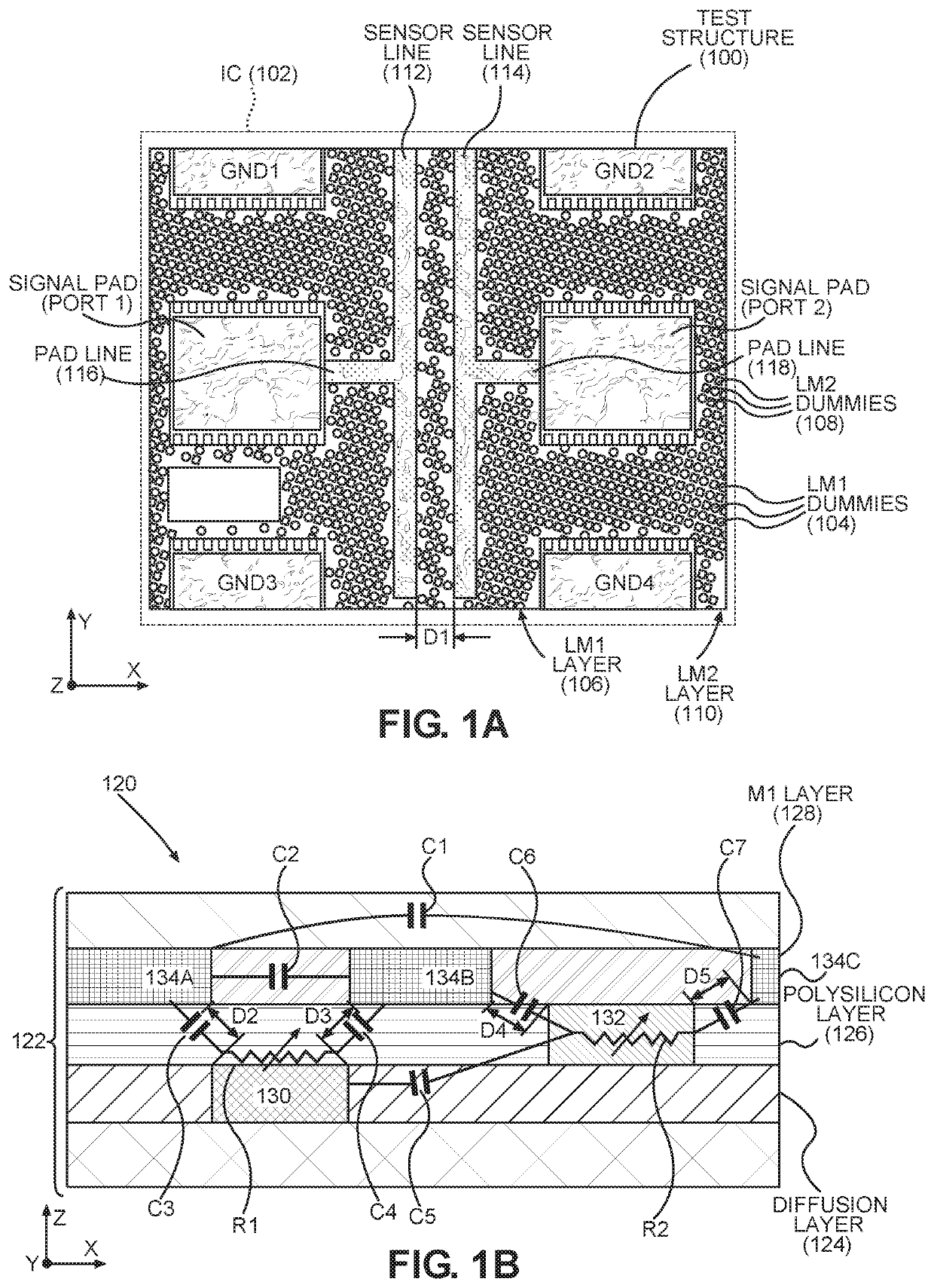
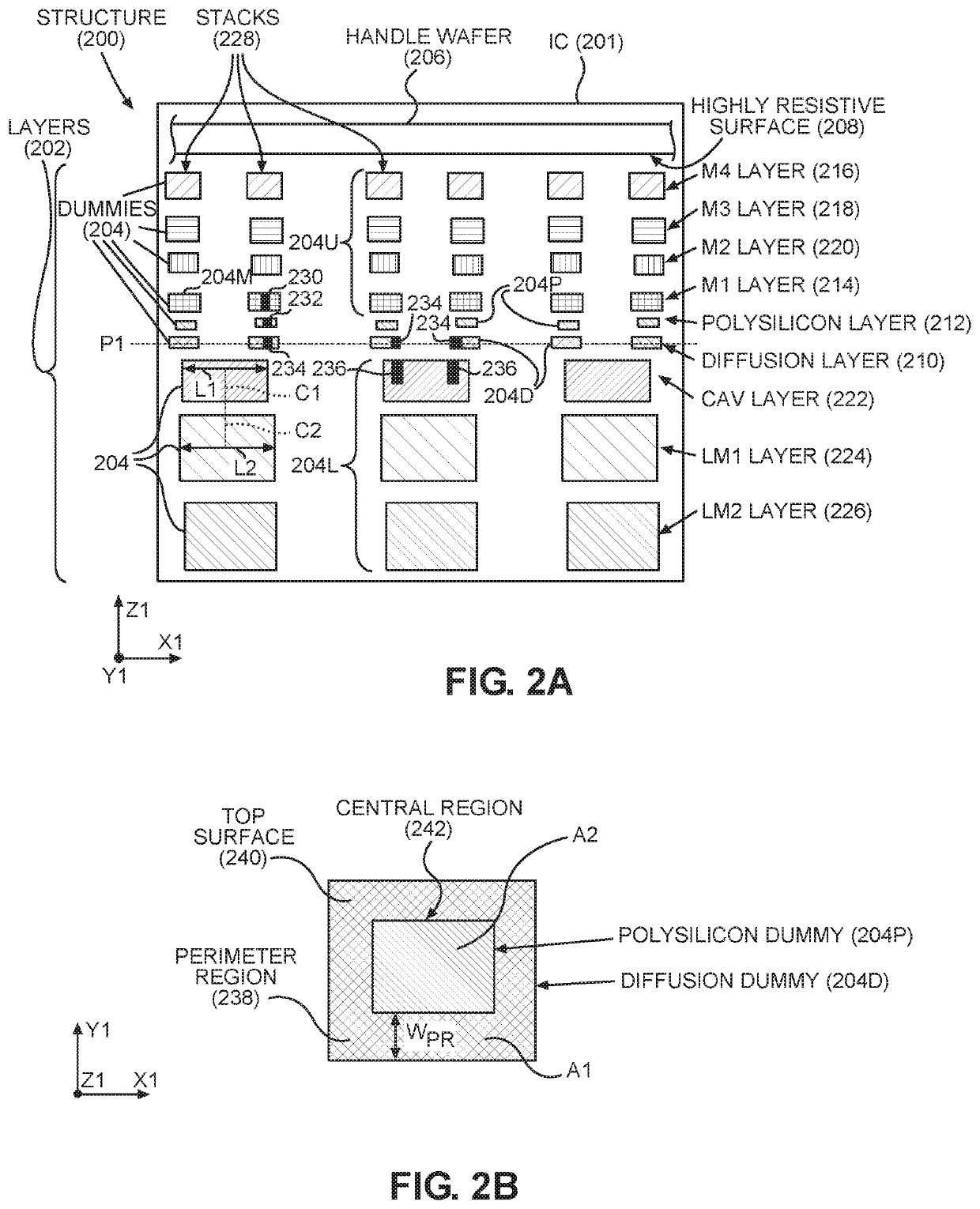
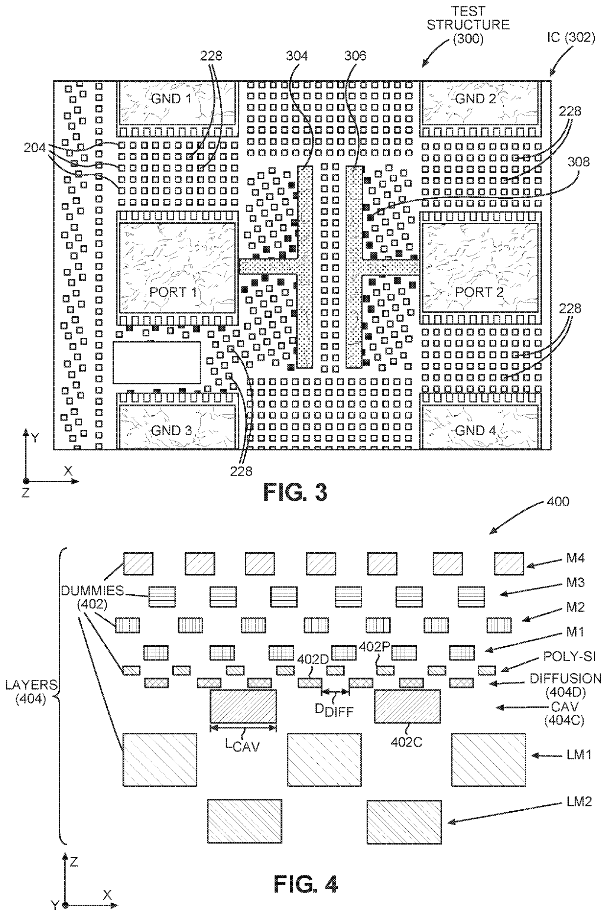
[0025]Aspects disclosed herein include vertically-aligned and conductive dummies in integrated circuit (IC) layers for capacitance reduction and bias independence. In other aspects, methods of manufacturing ICs including vertically-aligned and / or conductive dummies are disclosed. Dummies are isolated inactive islands or regions of material in the respective layers of ICs provided in areas that do not include circuit features to avoid non-uniform polishing (“dishing”). In one exemplary aspect, a disclosed IC includes a plurality of diffusion layer dummies of semiconductor material, and a plurality of polysilicon dummies in a polysilicon layer disposed ...


PUM


Abstract

Vertically-aligned and conductive dummies in integrated circuit (IC) layers reduce capacitance and bias independence. Dummies are islands of material in areas of metal and semiconductor IC layers without circuit features to avoid non-uniform polishing (“dishing”). Conductive diffusion layer dummies in a diffusion layer and conductive polysilicon dummies in a polysilicon layer above the diffusion layer reduce bias dependence and nonlinear circuit operation in the presence of an applied varying voltage. ICs with metal dummies vertically aligned in at least one metal layer above the polysilicon dummies and diffusion dummies reduce lateral coupling capacitance compared to ICs in which dummies are dispersed in a non-overlapping layout by a foundry layout tool. Avoiding lateral resistance-capacitance (RC) ladder networks created by dispersed dummies improves signal delays and power consumption in radio-frequency (RF) ICs.

Description

BACKGROUNDI. Field of the Disclosure[0001]The technology of the disclosure relates generally to integrated circuit (IC) fabrication and, more particularly, to IC parasitic coupling capacitance and linearity.II. Background[0002]Transistors in an integrated circuit (IC) chip are electrically coupled to each other and to external circuit contacts by metal wires or traces. The transistors are formed in semiconductor layers in a three-dimensional (3D) structure which also includes metal layers for forming the metal traces. As the 3D structure is formed layer by layer, portions of the transistors and metal traces are created as features of patterns in a series of photolithographic processes. Pattern features within each layer may be densely populated in some areas, depending on the IC design, such that there is a small distance between features, while other areas are only sparsely populated or devoid of such features. In these other areas, the distance between features is larger, and thes...

Claims


Application Information

Patent Timeline
IPC IPC(8): H01L23/64H01L21/84H01L23/00H01L27/12H01L29/66
CPCH01L23/642H01L21/84H01L23/562H01L27/1203H01L27/12H01L29/6659H01L23/66H01L27/0207H01L22/12
Inventor KOLEV, PLAMEN VASSILEVVEMULAPALLI, ANIL KUMARDEIG, MATTHEW
Owner QUALCOMM INC
Why Eureka
Try Eureka