Enhanced performance ultraconductive copper and process of making

Pending Publication Date: 2020-09-17
TYCO ELECTRONICS AMP GMBH +1
View PDF0 Cites 2 Cited by
  • Summary
  • Abstract
  • Description
  • Claims
  • Application Information

AI Technical Summary

Benefits of technology

[0016]Another aspect of the invention relates to a method of forming an ultraconductive copper composite having enhanced RF conductivity where the composite has at least three composite layers. The method comprises forming a first graphene layer on a first layer of copper to form a first composite layer. A second and third graphene layer are formed on opposing sides of the second copper layer to form the second composite layer. A fourth layer of graphene is formed on a third copper layer to form the third composite layer of the ultraconductive copper composite. Chemical vapor deposition is preferably used to deposit the graphene on the first, second and third layer of the copper. The three composite layers are then stacked so that the first graphene layer of the first composite layer abuts the second graphene layer of the second composite layer to form a first interface and the fourth graphene layer of the third composite layer abuts the third graphene layer of the second composite layer to form a second interface. At least one of the interfaces is sufficiently close to the surface of the ult

Problems solved by technology

However, none of these efforts have been focused on improving the RF conductivity of the ultraconductive copper materials.
Furthermore, the production of ultraconductive copper composite wire and tape is problematic leading to non-uniform, unpredictable results which often times are not reproducible.
In addition, the processing of such wire and tape is generally done in small batch processes with extremely low yields.
The report states that many processes that are being developed to produce ultraconductive materials do not produce shapes for commercial applications, such as wires.
T

Method used


Image

  • Enhanced performance ultraconductive copper and process of making
  • Enhanced performance ultraconductive copper and process of making
  • Enhanced performance ultraconductive copper and process of making

Examples


Example

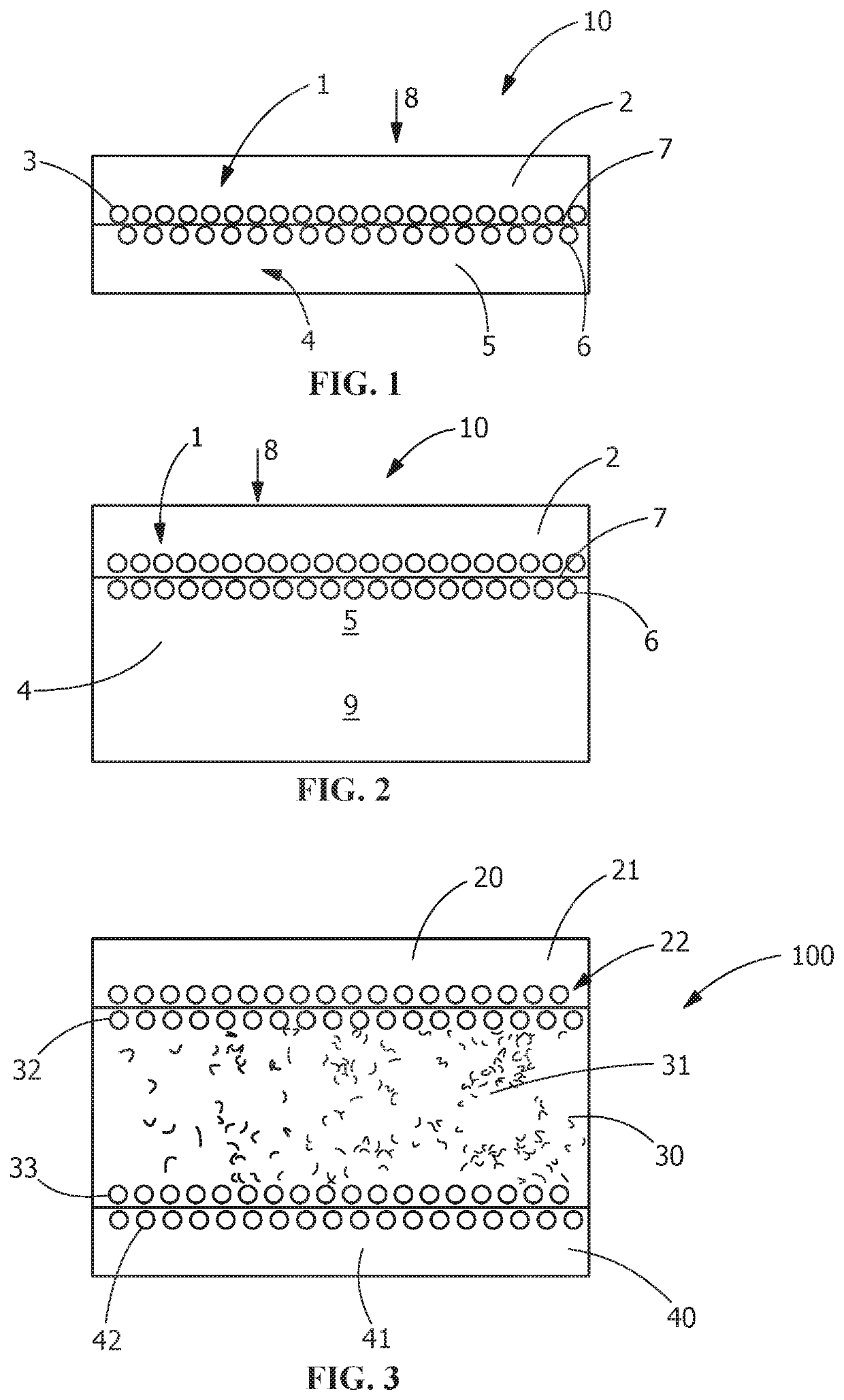
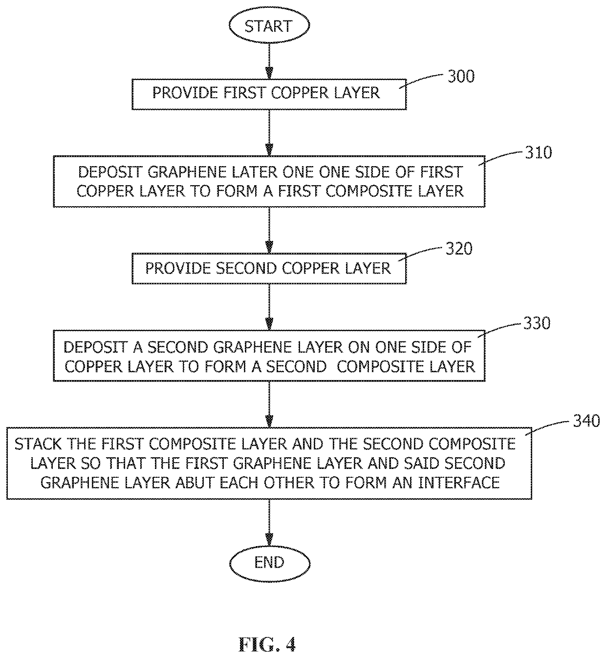
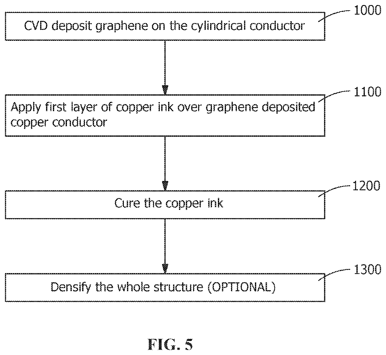
[0032]The description of illustrative embodiments according to principles of the present invention is intended to be read in connection with the accompanying drawings, which are to be considered part of the entire written description. In the description of embodiments of the invention disclosed herein, any reference to direction or orientation is merely intended for convenience of description and is not intended in any way to limit the scope of the present invention. Relative terms such as “lower,”“upper,”“horizontal,”“vertical,”“above,”“below,”“up,”“down,”“top” and “bottom” as well as derivative thereof (e.g., “horizontally,”“downwardly,”“upwardly,” etc.) should be construed to refer to the orientation as then described or as shown in the drawing under discussion. These relative terms are for convenience of description only and do not require that the apparatus be constructed or operated in a particular orientation unless explicitly indicated as such. Terms such as “attached,”“affi...


PUM

PropertyMeasurementUnit
Thicknessaaaaaaaaaa
Frequencyaaaaaaaaaa
Frequencyaaaaaaaaaa

Abstract

The present invention relates to an enhanced performance ultraconductive copper composite structure. The ultraconductive copper composite structure comprises at least two composite layers in which the interface between the two composite layers is sufficiently close to the surface of the ultraconductive copper composite so as to enhance the RF conductivity of the ultraconductive copper composite. The present invention also provides for method of forming such a ultraconductive copper composite structure.

Description

CROSS REFERENCE TO RELATED APPLICATIONS[0001]This non-provisional application claims the benefit under 35 U.S. Code § 119(e) of Provisional Application Ser. No. 62 / 817,118 filed Mar. 12, 2019 entitled ENHANCED PERFORMANCE ULTRACONDUCTIVE COPPER, Provisional Application Ser. No. 62 / 817,108 filed Mar. 12, 2019 entitled SYNTHESIS OF ULTRACONDUCTIVE METAL-CARBON COMPOSITES ON CYLINDRICAL SUBSTRATES and Provisional Application No. 62 / 817,102 filed Mar. 12, 2019 entitled REEL TO REEL PROCESS OF FORMING ULTRACONDUCTIVE METAL CARBON COMPOSITE WIRE AND TAPE AND USES THEREOF and whose entire disclosures are incorporated by reference herein.FIELD OF THE INVENTION[0002]The present invention is directed to a composite structure with graphene and copper that has improved RF conductivity. Furthermore, the invention relates to a method of making such a composite structure having improved RF conductivity.BACKGROUND OF THE INVENTION[0003]Copper is used for electrical and electronic purposes in the wo...

Claims


Application Information

Patent Timeline
IPC IPC(8): H01B1/02B32B15/20H01B1/04
CPCH01B1/04B32B15/20H01B1/026
Inventor BAYES, MARTIN W.BECKER, TOBIASWOLF, MARCOSANATI, SHAHROKHGULSOY, GOKCEWU, YILIANG
Owner TYCO ELECTRONICS AMP GMBH
Why Eureka
Try Eureka