

Laser removal of conductive seed layers
a technology of conductive seed layer and laser removal, which is applied in the direction of manufacturing tools, auxillary shaping apparatus, welding/soldering/cutting articles, etc., can solve the problems of increased process time and more expensive methodologies and equipment, undetectable higher cost of ownership, and limited process capability
- Summary
- Abstract
- Description
- Claims
- Application Information
AI Technical Summary
Benefits of technology
Problems solved by technology
Method used
Image

Examples
Embodiment Construction
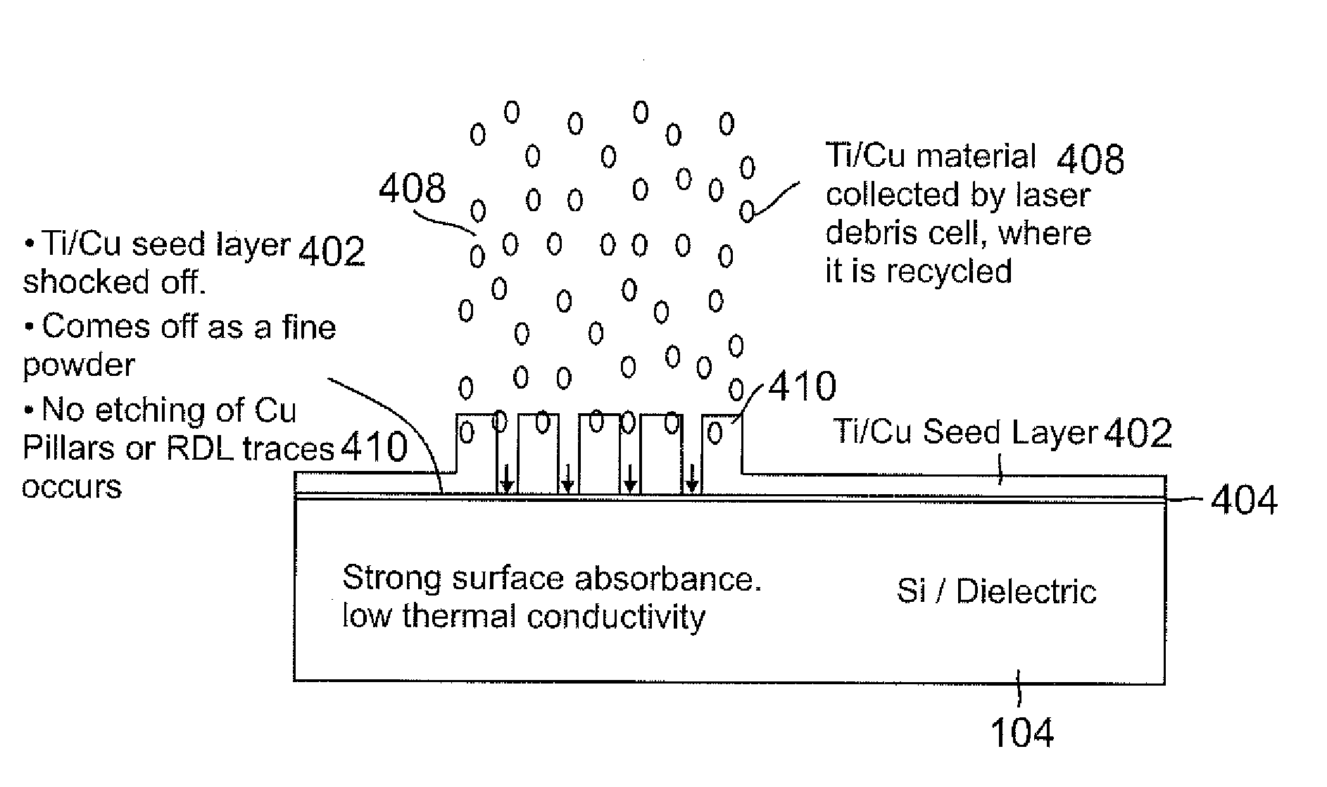
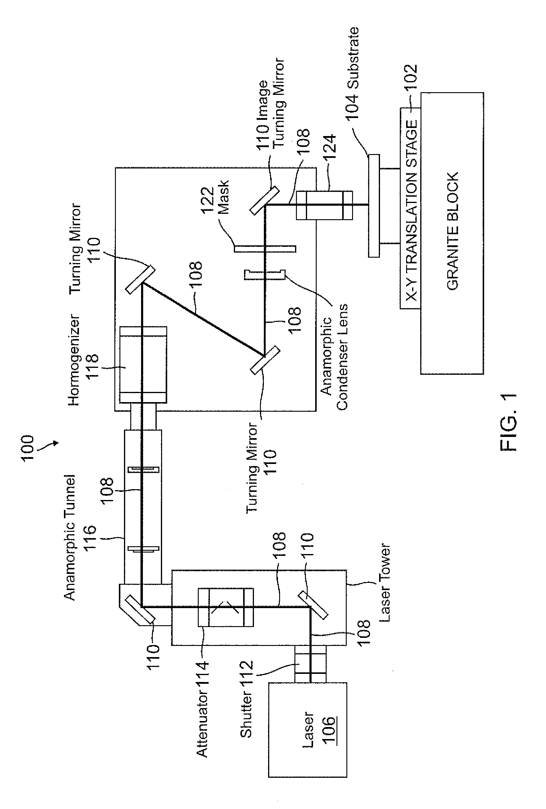
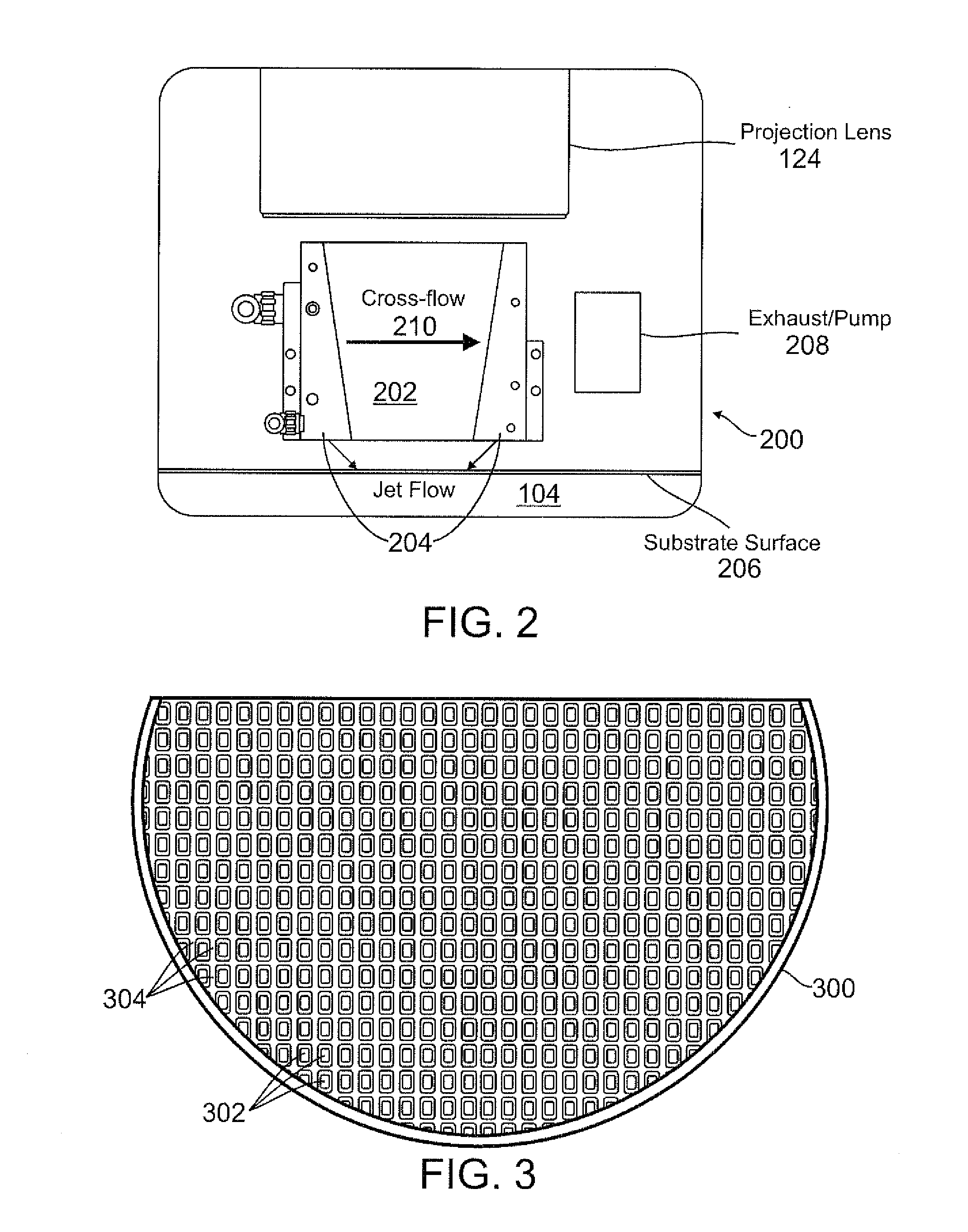
[0020]In the electrical substrate and wafer fabrication industry, the formation of conductive structures, e.g., traces, bonding pads, conductive bump interconnects, redistribution layer (RDL) traces, and the like, upon a surface of the substrate typically begins with the formation of a dielectric or electrically insulating layer on a “working” or “active” surface of the substrate. The insulating layer can comprise a polymer, such as a polyimide, or polybenzobisoxazole or “PBO,” e.g., HD8930, HD8820 or HD4100, all available from HD MicroSystems (http: / / hdmicrosystems.com), which can be deposited onto the substrate, for example, by a spinning operation. Alternatively, another type of insulator, such as silicon dioxide (SiO2) or silicon nitride (SiNx), can be formed on the substrate, such as a silicon wafer, using well-known oxidization techniques.
[0021]Following this, a “seed layer” of, e.g., Cu, Ti / Cu, TiW / Cu, Ti, CrCu, Ni, Pd or the like, is deposited over the insulating layer on th...
PUM
| Property | Measurement | Unit |
|---|---|---|
| thickness | aaaaa | aaaaa |
| thickness | aaaaa | aaaaa |
| thickness | aaaaa | aaaaa |
Abstract
Description
Claims
Application Information