Multichip Packages

a technology of multi-chip packages and chips, applied in the direction of semiconductor devices, semiconductor/solid-state device details, electrical apparatus, etc., can solve the problems of significant challenges in manufacturability and structural reliability

Inactive Publication Date: 2012-08-02
MEGIT ACQUISITION
View PDF4 Cites 333 Cited by
  • Summary
  • Abstract
  • Description
  • Claims
  • Application Information

AI Technical Summary

Problems solved by technology

While WLP is a high throughput and low cost approach to IC chip packaging, it however invites significant challenges in manufacturability and structural reliability.

Method used


Image

  • Multichip Packages
  • Multichip Packages
  • Multichip Packages

Examples


Embodiment Construction

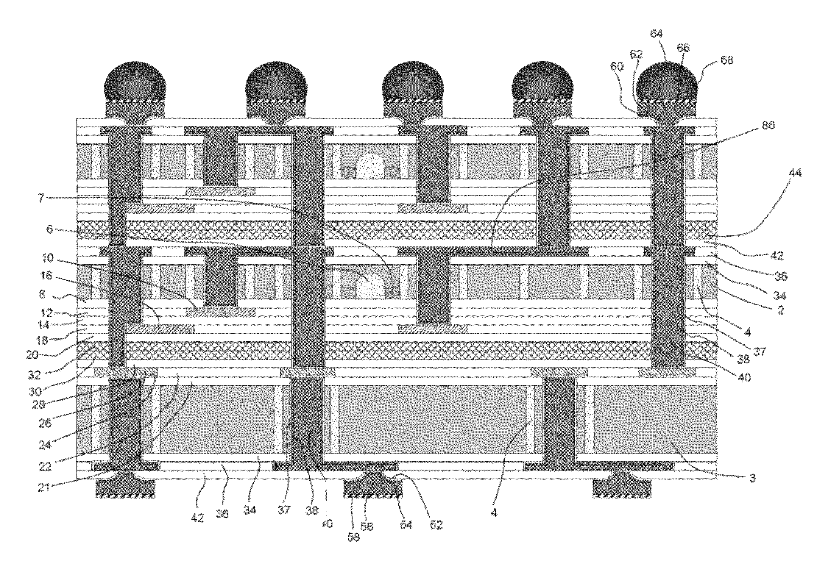
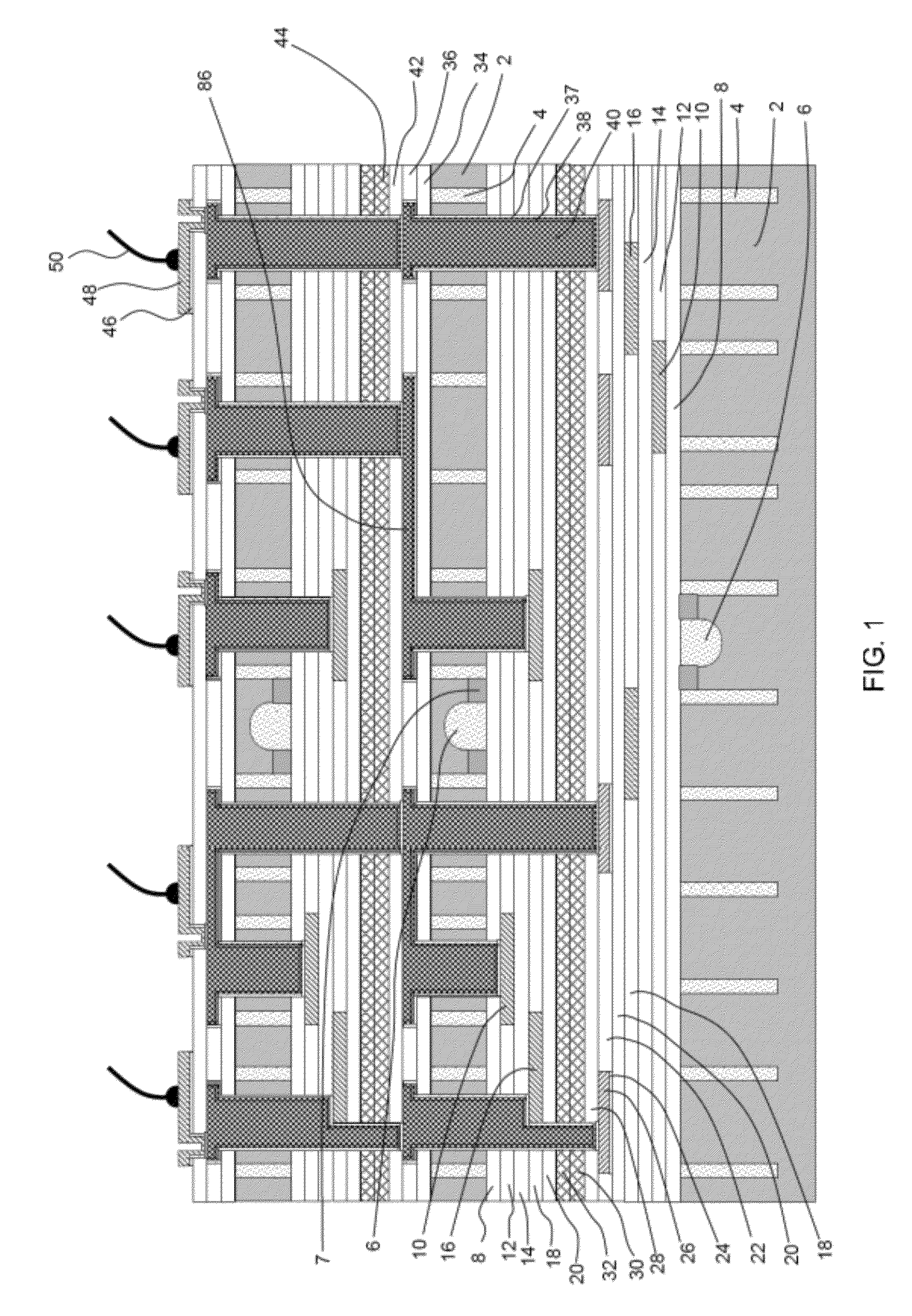
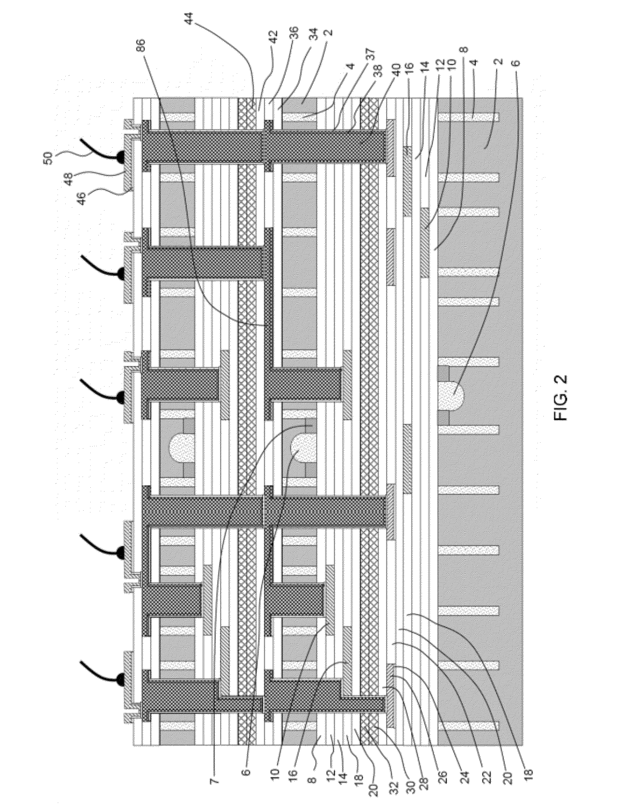
[0040]Illustrative embodiments are now described. Other embodiments may be used in addition or instead. Details that may be apparent or unnecessary may be omitted to save space or for a more effective presentation. Conversely, some embodiments may be practiced without all of the details that are disclosed.

[0041]The process of fabricating multichip packages described herein may include fabricating isolation enclosures and through silicon / substrate vias (TSVs) using enclosure-first technology. Enclosure-first technology may include forming an isolation enclosure associated with a TSV early in the fabrication process, without actually forming the associated TSV. The TSV associated with the isolation enclosure is formed later in the fabrication process. Deep trenches may be formed to provide TSV isolation, while shallow trenches may be formed for active device isolation. The enclosure-first technology may also allow the isolation enclosures to be used as alignment marks for additional w...


PUM


Abstract

Multichip packages or multichip modules may include stacked chips and through silicon / substrate vias (TSVs) formed using enclosure-first technology. Enclosure-first technology may include forming an isolation enclosure associated with a TSV early in the fabrication process, without actually forming the associated TSV. The TSV associated with the isolation enclosure is formed later in the fabrication process. The enclosure-first technology allows the isolation enclosures to be used as alignment marks for stacking additional chips. The stacked chips can be connected to each other or to an external circuit such that data input is provided through the bottom-most (or topmost) chip, data is output from the bottom-most (or topmost) chip. The multichip package may provide a serial data connection, and a parallel connection, to each of the stacked chips.

Description

[0001]This application claims priority to U.S. Provisional Application No. 61 / 438,635, filed on Feb. 1, 2011, which is incorporated herein by reference.BACKGROUND OF THE DISCLOSURE[0002]1. Field of the Disclosure[0003]The disclosure relates to multichip packages, and more particularly, to multichip packages that include through substrate / silicon vias (TSVs) formed in stacked chips using enclosure-first technology and / or in stacked wafers, such as stacked Flash memory chips.[0004]2. Brief Description of the Related Art[0005]Semiconductor wafers are processed to produce IC (integrated circuit) chips having ever-increasing device density and shrinking feature geometries. Multiple conductive and insulating layers are required to enable the interconnection and isolation of the large number of semiconductor devices in different layers. Such large scale integration results in an increasing number of electrical connections between various layers and semiconductor devices. It also leads to a...

Claims


Application Information

Patent Timeline
Patent Type & Authority Applications(United States)
IPC IPC(8): H01L23/498
CPCH01L2224/9202H01L2924/01005H01L2924/01006H01L2924/01019H01L2924/01023H01L2924/01024H01L2924/01033H01L2924/01072H01L2924/01074H01L2924/01077H01L2924/01087H01L2924/014H01L2224/48624H01L2224/05569H01L24/16H01L24/92H01L2224/0345H01L2224/03462H01L2224/0401H01L2224/04042H01L2224/05008H01L2224/05558H01L2224/05624H01L2224/05655H01L2224/13111H01L2224/16225H01L2224/2919H01L2224/05572H01L2924/01014H01L2924/01028H01L2224/48724H01L2224/48599H01L2224/48799H01L2224/48091H01L2224/48147H01L2224/48463H01L2924/01015H01L2924/00014H01L21/76229H01L21/76898H01L23/481H01L24/05H01L24/13H01L24/29H01L24/32H01L24/45H01L24/48H01L24/80H01L24/83H01L24/94H01L24/97H01L25/0657H01L25/50H01L2221/6835H01L2221/68377H01L2223/54426H01L2224/05009H01L2224/05187H01L2224/0557H01L2224/08145H01L2224/29187H01L2224/32145H01L2224/45124H01L2224/45144H01L2224/45147H01L2224/48227H01L2224/80896H01L2224/8385H01L2224/83896H01L2224/94H01L2224/97H01L2225/0651H01L2225/06517H01L2225/06541H01L2225/06544H01L2225/06562H01L2924/01013H01L2924/01029H01L2924/01032H01L2924/01047H01L2924/01049H01L2924/01057H01L2924/01058H01L2924/01073H01L2924/01079H01L2924/01082H01L2924/09701H01L2924/10253H01L2924/10271H01L2924/10329H01L2924/10335H01L2924/12036H01L2924/1205H01L2924/1206H01L2924/1207H01L2924/1436H01L2924/1437H01L2924/1438H01L2924/1441H01L2924/1451H01L2924/14511H01L2924/15311H01L2224/80H01L2224/83H01L2924/01046H01L2924/00H01L2224/05552H01L2924/15787H01L2924/15788H01L2224/48655H01L2224/48824H01L2224/48855H01L2224/48755H01L2224/48145H01L2924/00011H01L2224/9212H01L2224/8203H01L2224/821H01L2224/80001H01L2224/82
Inventor LIN, MOU-SHIUNGYANG, PING-JUNGLO, HSIN-JUNGLIU, TE-SHENGLEE, JIN-YUAN
Owner MEGIT ACQUISITION
Why Eureka
Try Eureka