Eureka AIR delivers breakthrough ideas for toughest innovation challenges, trusted by R&D personnel around the world.

Liquid crystal display device

a liquid crystal display and display device technology, applied in the direction of fire alarm mechanical actuation, signaling system, instruments, etc., can solve the problems of deteriorating image quality, ghost image appearance, and easy damage to the upper polarizing plate, and achieve good contrast and prevent light leakage in the margins

Active Publication Date: 2012-08-09
JAPAN DISPLAY INC
View PDF6 Cites 12 Cited by
  • Summary
  • Abstract
  • Description
  • Claims
  • Application Information

AI Technical Summary

Benefits of technology

[0011]In fact, in the structure in which the front window 30 and the liquid crystal display panel are bonded with the bonding material 40, as shown in FIG. 7, a problem is the incoming light through the chamfered edges of the front window 30. In the structure in which the front window 30 is attached to the liquid crystal display panel with the bonding material 40, the present invention is intended to prevent light from the backlight 200 or external light from entering the margins of the front window 30 and to prevent contrast deterioration in the margins of the screen when the viewing angle is wide.
[0014]According to the present invention, in a liquid crystal display device having a front window, it is possible to block out light of a backlight that enters the front window through its chamfers. Hence, it is possible to prevent light leakage in the margins of the screen when the screen is viewed obliquely. Thus, a liquid crystal display device that provides a good contrast, even if the screen is viewed from an oblique direction, can be achieved.

Problems solved by technology

An upper polarizing plate is attached to the upper surface of the opposing substrate and the upper polarizing plate is prone to damage because it is made of resin.
In the case of related art as typified in FIG. 8, a problem of ghost image appearance arises. FIG. 8 is an explanatory diagram about ghost image appearance, taking a reflective liquid crystal display panel as an example.
This phenomenon of ghost image appearance deteriorates image quality.
Another problem that is encountered by a liquid crystal display panel is that light is reflected from the edge faces of the TFT substrate 10 and the opposing substrate 20 and radiated from the display region, which degrades the contrast of the screen.

Method used


Image

  • Liquid crystal display device
  • Liquid crystal display device
  • Liquid crystal display device

Examples


first embodiment

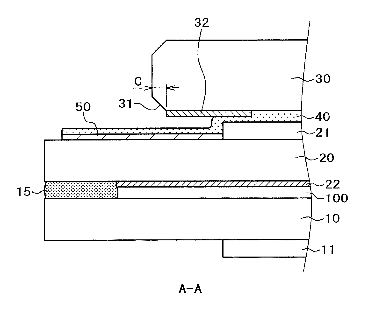
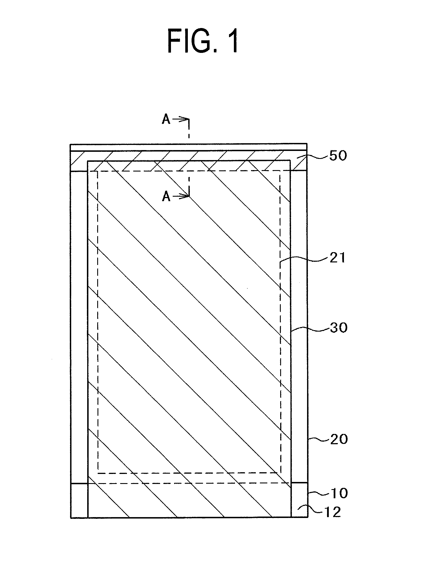
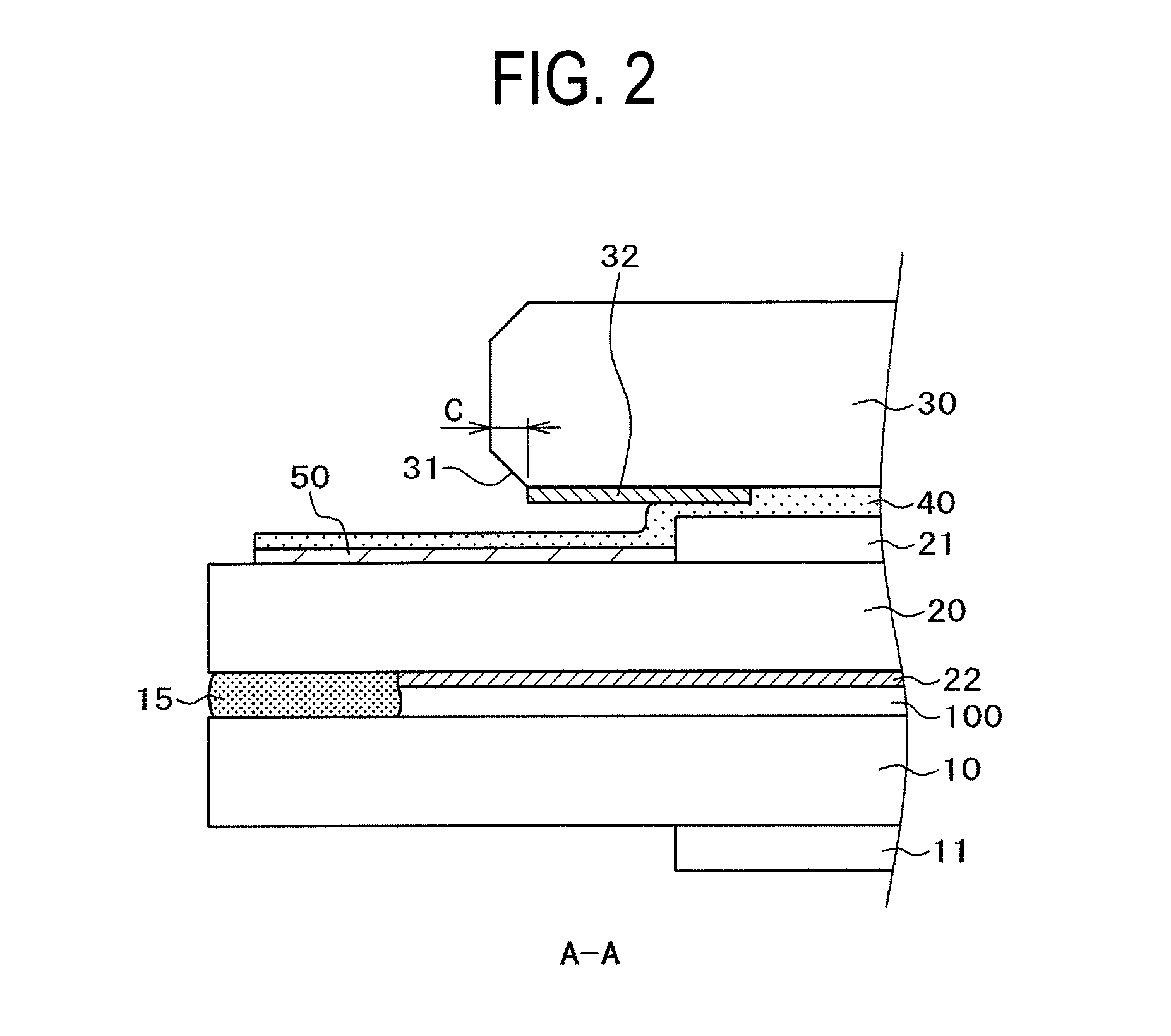
[0026]FIG. 1 is a plan view representing a first embodiment of the present invention and FIG. 2 is a cross-sectional view taken along line A-A in FIG. 1. In FIG. 1, a liquid crystal display panel is formed by a TFT substrate 10 and an opposing substrate 20. A lower polarizing plate 11 is attached to the TFT substrate 10, while an upper polarizing plate 21 is attached to the upper surface of the opposing substrate 20. A backlight 200 is located under the TFT substrate 10. The TFT substrate 10 is formed larger than the opposing substrate 20. A region where the TFT substrate 10 only extends is a terminal section 12 in which an IC driver and other components, which are not shown, are installed.

[0027]On top of the liquid crystal display panel and the upper polarizing plate 21, a front window 30 made of glass is attached. In FIG. 1, the outlines of the front window 30, its three sides with the exception of a side congruent with the terminal section 12 of the liquid crystal display panel, ...

second embodiment

[0037]FIG. 4 is a plan view of a liquid crystal display device according to a second embodiment of the present invention and FIG. 5 is a cross-sectional diagram through line B-B in FIG. 4. In FIG. 4, a difference from FIG. 1 is that a (frame-like) light shielding tape 60 shaped for marginal edges is formed around the front window 30. The inner edges of the light shielding tape 60 shaped for marginal edges coincide with the outer edges of the front window 30. Other structural details are the same as those in FIG. 1.

[0038]FIG. 5 is a cross-sectional diagram through line B-B in FIG. 4. FIG. 5 differs from FIG. 2 in that the light shielding tape 60 shaped for marginal edges is formed around the front window 30. The inner edges of the light shielding tape 60 shaped for marginal edges coincide with the outer edges of the front window 30. The light shielding tape 60 shaped for marginal edges serves to block out light from the backlight that is leaked from the edge portions of the opposing ...

third embodiment

[0042]FIG. 10 is a cross-sectional view representing another embodiment of the present invention. In FIG. 10, the liquid crystal display panel and the backlight 200 are accommodated within a mold 110 and this mold 110 is accommodated with the bottom frame 120. In FIG. 2, FIG. 5, FIG. 7, etc. the mold 110 is excluded for convenience sake. In this embodiment, by providing the light shielding material 50 directly on the upper surface of the opposing substrate 20 in its margins, light from the backlight 200, as indicated by an arrow, is prevented from being emitted through the upper surface of the opposing substrate 20.

[0043]A major difference between this embodiment and the preceding embodiments is that the light shielding material 50 is attached below the polarizing plate 21. In addition, the light shielding material 50 and the polarizing plate 21 are placed overlapping each other. The light shielding material 50 may be provided by tape attachment or print in the structure. In order t...


PUM


Abstract

In a liquid crystal display device having a front window, light from a backlight is prevented from leaking through chamfered edges of the front window. An upper polarizing plate is formed on an opposing substrate and a light shielding material is formed abutting on an outer edge of the upper polarizing plate. Edges of the upper polarizing plate are located inward of edges of the front window. The upper polarizing plate and the front window are bonded with a boding material including an ultraviolet curable resin. The ultraviolet curable resin also lies over the light shielding material. Chamfers are formed in the front window and the ultraviolet curable resin does not adhere to the chamfers of the front window. By this structure, light from the backlight is prevented from entering the internal part of the front window through the chamfers of the front window and light leakage is prevented.

Description

CLAIM OF PRIORITY[0001]The present application claims priority from Japanese Patent Application JP 2011-023917 filed on Feb. 7, 2011, the content of which is hereby incorporated by reference into this application.FIELD OF THE INVENTION[0002]The present invention relates to a liquid crystal display device and particularly to a technique for improving the strength and visibility of a miniature display device for use in a digital still camera, a cell phone, etc.BACKGROUND OF THE INVENTION[0003]In a liquid crystal display device, a TFT substrate over which pixel electrodes and thin-film transistors (TFTs), inter alia, are formed in a matrix and an opposing substrate over which color filters, inter alia, are formed in positions corresponding to the pixel electrodes in the TFT substrate are placed facing each other and liquid crystals are sandwiched between the TFT substrate and the opposing substrate. An image is produced by controlling light transmissibility through liquid crystal molec...

Claims


Application Information

Patent Timeline
IPC IPC(8): G02F1/1335G02F1/1368
CPCG02F1/133308G02F1/133512G02F2202/28G02F2202/023G02F2001/133331G02F1/133331G08B3/1025G08B17/02G08B17/06
Inventor HARAYAMA, TAKESHIYOSHIMOTO, TAKASHIISHII, KATSUHIKOKOBAYASHI, SETSUOISHII, AKIRATANABE, SHINJISENTO, KIYOSHI
Owner JAPAN DISPLAY INC
Why Eureka
Eureka Blog
Learn More