Fault-tolerant unit and method for through-silicon via

a technology of through-silicon via and fault-tolerant unit, which is applied in the direction of semiconductor/solid-state device testing/measurement, semiconductor device details, semiconductor/solid-state device testing/measurement, etc., can solve the problem that 3d ic cannot normally work

Active Publication Date: 2012-10-04
IND TECH RES INST
View PDF6 Cites 27 Cited by
  • Summary
  • Abstract
  • Description
  • Claims
  • Application Information

AI Technical Summary

Benefits of technology

[0010]According to the above descriptions, the TSV structures TSV1-TSVn having the same signal characteristic in the chip stacking structure are used to form a fault-tolerant unit, and the fault-tolerant unit is unnecessary to add additional TSV structures. Namely, in the normal operation state, the TSV structures TSV1-TSVn respectively transmit a plurality of signals (for example, clock signals) having the same characteristic from the first chip to a plurality of circuit modules (for example, clock trees) of the second chip. When the TSV structure TSVi is faulty and cannot transmit a signal to the node N2i of the second chip, the switch module can transmit a signal (a signal having the same characteristic) of the other TSV structure to the node N2i. Therefore, the fault-tolerant unit of the disclosure may have a TSV fault tolerant effect.

Problems solved by technology

However, once the TSV structure is faulty, the 3D IC cannot normally work due to failure of signal transmission.

Method used


Image

  • Fault-tolerant unit and method for through-silicon via
  • Fault-tolerant unit and method for through-silicon via
  • Fault-tolerant unit and method for through-silicon via

Examples


Embodiment Construction

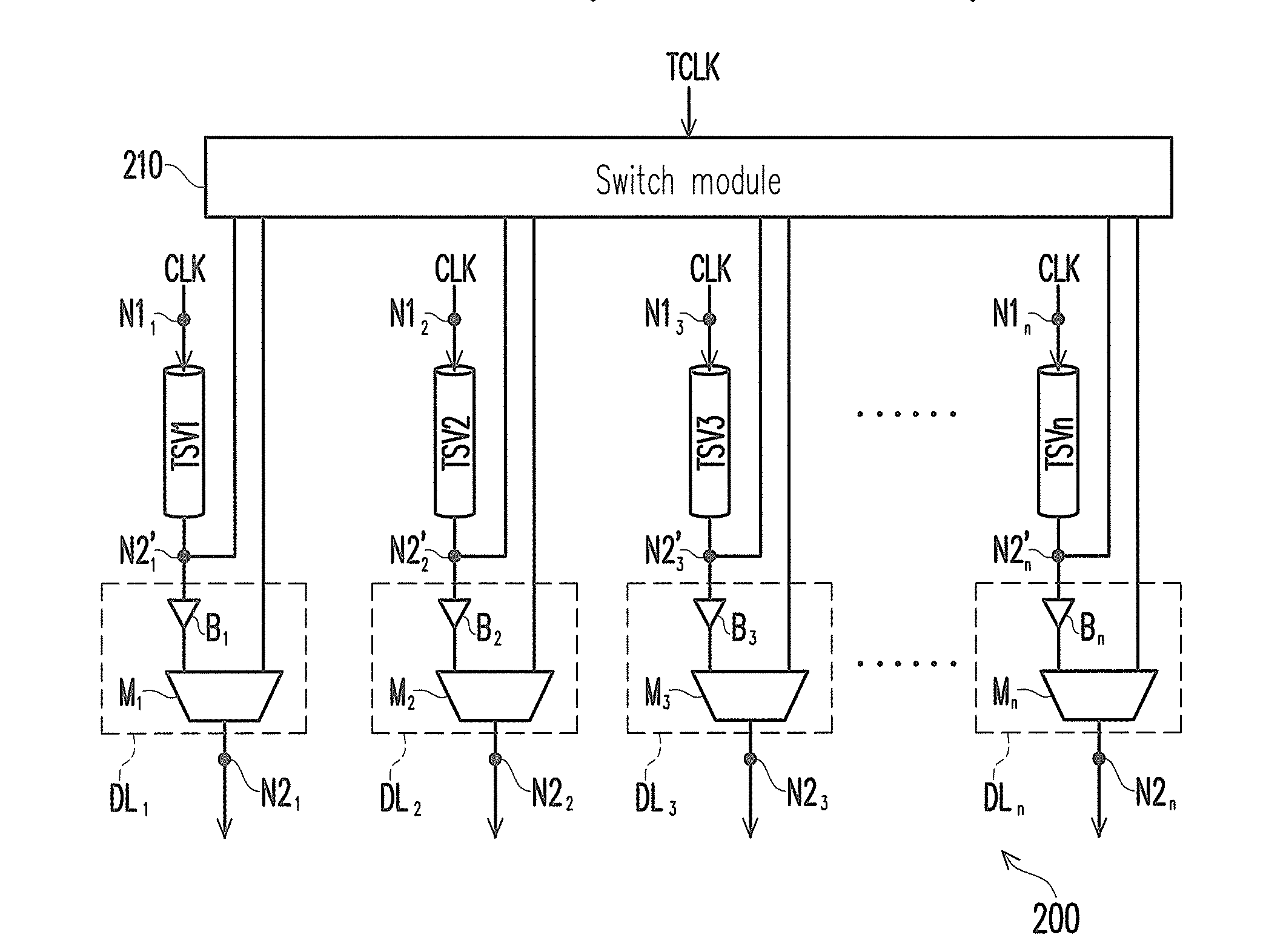
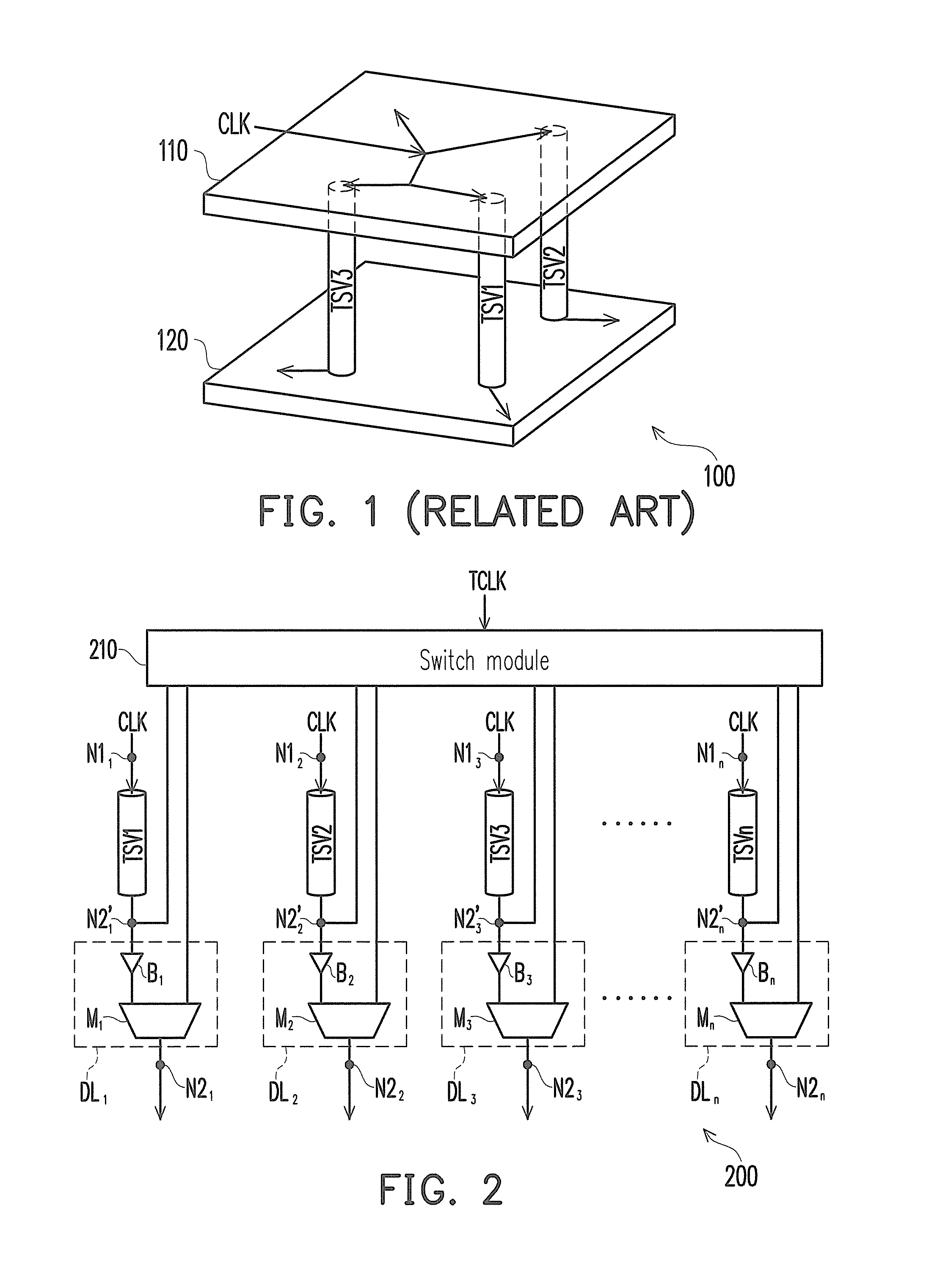
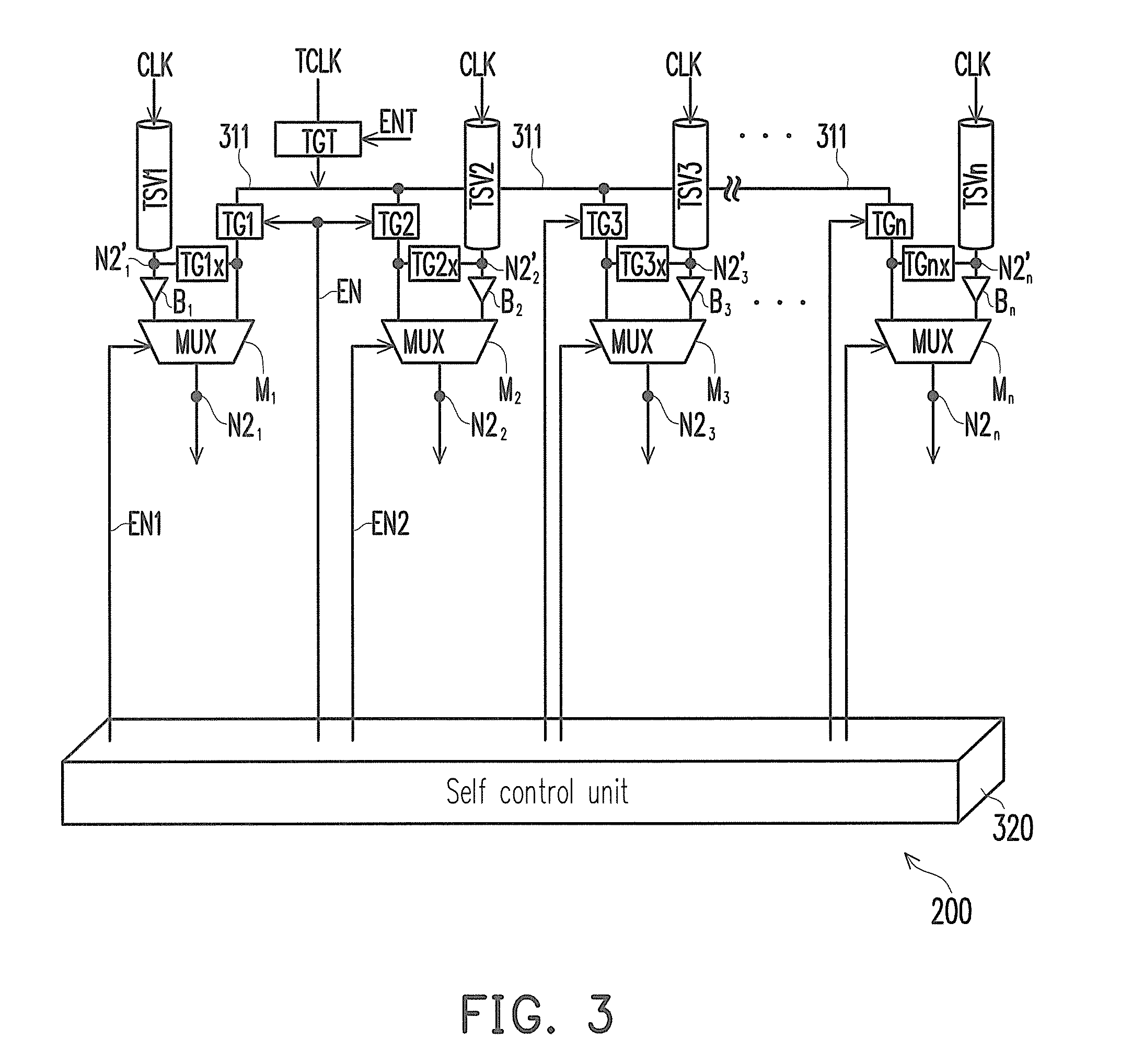
[0024]FIG. 2 is a functional block schematic diagram of a fault-tolerant unit for through-silicon via (TSV) according to an exemplary embodiment of the disclosure. The fault-tolerant unit 200 for TSV includes n TSV structures (for example, TSV1, TSV2, TSV3, TSVn in FIG. 2), n first nodes (for example, N11, N12, N13, . . . , Nn in FIG. 2), n second nodes (for example, N21, N22, N23, . . . , N2n in FIG. 2), and a switch module 210, where n is an integer. The first nodes N11-N1n, are disposed on a first chip of a chip stacking structure, and the second nodes N21-N2n are disposed on a second chip of the chip stacking structure, where the first chip is stacked on the second chip. After the first chip is stacked on the second chip, the TSV structure TSVi is electrically connected between the first node N1i and the second node N2i, where 1≦i≦n.

[0025]The switch module 210 is disposed on the second chip. The switch module 210 is connected between the second nodes N21-N2n and a test path of t...


PUM


Abstract

A fault-tolerant unit and a fault-tolerant method for through-silicon via (TSV) are provided. The fault-tolerant unit includes TSV structures TSV1˜TSVn, nodes N11˜N1n, nodes N21˜N2n and a switching module. The TSV structure TSVi is connected between the node N11 of the first chip and the node N2i of the second chip, wherein 1≦i≦n. The switching module is connected between the nodes N21˜N2n of the second chip and a test path of the second chip. In normal operation state, the switching module disconnects the test path and the nodes N21˜N2n when the TSV structures TSV1˜TSVn are valid. The switching module connects the node N2i to at least another one of the nodes N21˜N2n when the TSV structure TSVi is faulty in the normal operation state. In test status, the switching module connects the test path to the nodes N21˜N2n.

Description

CROSS-REFERENCE TO RELATED APPLICATION[0001]This application claims the priority benefits of U.S. provisional application Ser. No. 61 / 468,078, filed on Mar. 28, 2011 and Taiwan application serial no. 100120191, filed on Jun. 9, 2011. The entirety of each of the above-mentioned patent applications is hereby incorporated by reference herein and made a part of this specification.BACKGROUND[0002]1. Technical Field[0003]The disclosure relates to a chip stacking structure having through-silicon vias (TSVs). Particularly, the disclosure relates to a fault-tolerant unit and a fault-tolerant method for TSV.[0004]2. Related Art[0005]A three-dimensional (3D) integrated circuit (IC) is a chip stacking structure formed by stacking a plurality of chips. FIG. 1 is a schematic diagram of a conventional chip stacking structure. The chip stacking structure 100 includes a chip 110 and a chip 120, and a plurality of through-silicon via (TSV) structures is disposed between the chip 110 and the chip 120....

Claims


Application Information

Patent Timeline
Patent Type & Authority Applications(United States)
IPC IPC(8): H01L23/58H01L21/66
CPCH01L23/481H01L2224/16146H01L2225/06544H01L25/0657
Inventor LUNG, CHIAO-LINGSU, YU-SHIHCHANG, SHIH-CHIEHSHI, YIYU
Owner IND TECH RES INST
Why Eureka
Try Eureka