Bending sensor and method for fabricating the same

a technology of bending sensor and bending direction, applied in the direction of resistors adapted for applying terminals, resistance/reactance/impedence, instruments, etc., can solve the problem of not being able to sense the degree and direction of folding or bending in the hole-sensor based structure, and the limitation of the display device's size to support multimedia functions,

Inactive Publication Date: 2012-10-11
SAMSUNG ELECTRONICS CO LTD
View PDF7 Cites 72 Cited by
  • Summary
  • Abstract
  • Description
  • Claims
  • Application Information

AI Technical Summary

Benefits of technology

[0013]Accordingly, an aspect of the present invention is to provide a bending sensor, which can sense the degree and direction of folding or bending of a flexible display device while limiting the need to increase the flexible display device in size, and a method for fabricating the bending sensor.
[0014]Another aspect of the present invention is to provide a bending sensor which can variously control a flexible display element by sensing the degree and direction of folding or bending of the flexible display element, and a method for fabricating the bending sensor.

Problems solved by technology

However, in terms of portability of the portable terminal, there is a limitation in increasing the size of the display device to support the multimedia functions.
In other words, as the thickness of the flexible display element increases, a displacement on the inner surface or the outer surface also increases during the folding or bending operation, involving some risk of damage to the flexible display element.
However, the hole-sensor based structure can sense deformation only under particular conditions, for example, deformation such as the rolling or folding of the flexible display element is generated only in the direction of the hole sensors.
Moreover, the hole-sensor based structure cannot sense the degree and direction of folding or bending.

Method used


Image

  • Bending sensor and method for fabricating the same
  • Bending sensor and method for fabricating the same
  • Bending sensor and method for fabricating the same

Examples


Embodiment Construction

[0032]Hereinafter, embodiments of the present invention will be described in detail with reference to the accompanying drawings. A detailed description of known functions and configurations will be omitted when it may unnecessarily obscure the subject matter of the present invention.

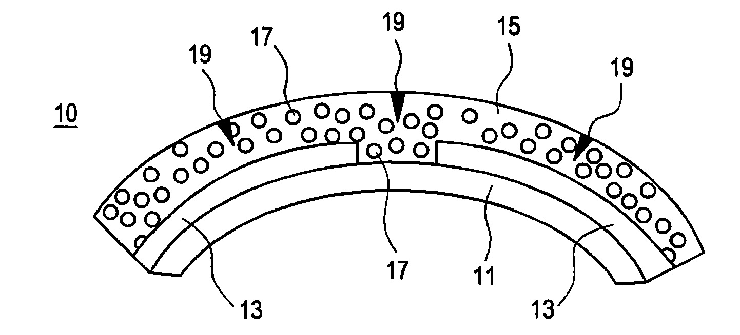
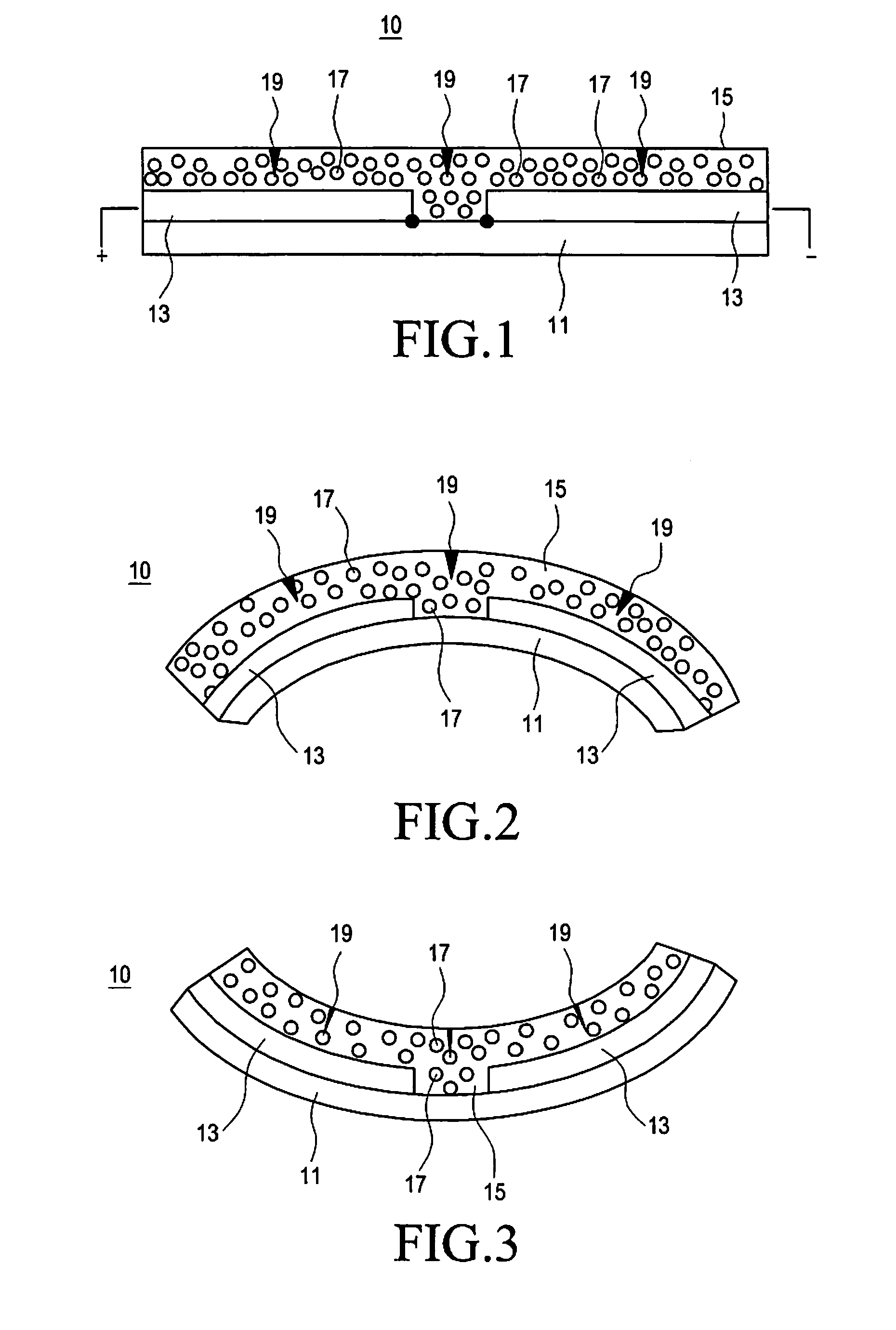
[0033]As shown in FIGS. 1 through 3, a bending sensor 10 according to an embodiment of the present invention is structured such that at least a pair of electrode patterns 13 are disposed spaced apart from each other on a flexible substrate 11 and a paste layer 15 is formed to cover the electrode patterns 13. The paste layer 15 may be formed with paste containing conductive particles 17 or through ink printing or screen-printing. As shown in FIGS. 2 and 3, as a distance between the electrode patterns 13 changes due to deformation of the flexible substrate 11, the density of the conductive particles 17 distributed between the electrode patterns 13 also changes. Such a change leads to a change in an electri...


PUM

PropertyMeasurementUnit
flexibleaaaaaaaaaa
densityaaaaaaaaaa
electric resistanceaaaaaaaaaa

Abstract

A bend-detecting (bending) sensor is provided, including a flexible substrate, at least a pair of electrode patterns spaced apart from each other provided on the flexible substrate, and a paste layer containing conductive particles. The paste layer is coated onto the flexible substrate where the electrode patterns are formed, such that when the flexible substrate is bent, the density of the conductive particles between the electrode patterns changes and an electric resistance between the electrode patterns also changes, thereby sensing deformation of the flexible substrate, and eventually, a target to which the flexible display element or the flexible substrate is attached. When the bending sensor is applied to the flexible display device, the electrode patterns and the paste layer may be formed on the flexible substrate which is to form the flexible display element, thus forming a bending sensing structure with a thickness of the flexible display element or less.

Description

PRIORITY[0001]This application claims priority under 35 U.S.C. §119(a) to a Korean Patent Application filed in the Korean Intellectual Property Office on Apr. 8, 2011 and assigned Serial No. 10-2011-0032828, the contents of which are hereby incorporated by reference.BACKGROUND OF THE INVENTION[0002]1. Field of the Invention[0003]The present invention relates generally to a bending sensor and a method for fabricating the same, and more particularly to a bending sensor which is easily applicable to a flexible display device, and a method for fabricating the bending sensor.[0004]2. Description of the Related Art[0005]Generally, a display device refers to a device having a screen which provides image signal. The display device has been widely used in daily life for not only portable terminals, such as cellular phones, Portable Multimedia Players (PMPs), etc., but also electric appliances, such as navigation systems for vehicles, TVs, laundry machines, refrigerators, etc.[0006]With the c...

Claims


Application Information

Patent Timeline
Patent Type & Authority Applications(United States)
IPC IPC(8): G01L1/22H01C17/28
CPCG01L1/20H01C17/281G01L1/205H01C10/10G06F3/045H01C17/065G01B7/18Y10T29/49103G06F2203/04102G01B7/16G01R27/00
Inventor BYUN, KANG-HOKIM, BYUNG-JIK
Owner SAMSUNG ELECTRONICS CO LTD
Why Eureka
Try Eureka