Multi-layer adhesive assemblies for electronic devices

a technology of electronic devices and adhesive assemblies, applied in the field of assemblies, can solve the problems of difficult manufacturing, heavy or bulky arrangements, high cost, etc., and achieve the effect of improving the quality of the product, improving the service life, and improving the service li

Inactive Publication Date: 2012-11-01
APPLE INC
View PDF25 Cites 31 Cited by
  • Summary
  • Abstract
  • Description
  • Claims
  • Application Information

AI Technical Summary

Benefits of technology

[0007]The invention pertains to techniques or processes for producing assemblies using adhesives and substrate material, such as glass. In one embodiment, the assemblies may be for portable electronic devices. For example, a cover glass of a portable electronic device may have a first layer of a self-leveling adhesive, which may be adhesively coupled with the cover glass. A second layer of a second adhesive, which may be different than the self-leveling adhesive of the first layer, may be adhesively coupled with the first layer. An optical component may be adhesively coupled with the second layer, so as to secure the optical component. The first layer may be cured prior to securing the optical component, so that the optical component may be substantially isolated from stress effects of adhesive cure shrinkage of the first layer. Flexure, warpage or optical distortion of the optical component due to adhesive cure shrinkage may be substantially avoided.
[0013]As an assembly method, another embodiment can, for example, include at least forming a first layer of a first adhesive on a substrate, curing the first layer of the first adhesive, and substantially isolating an assembly component from stress of adhesive cure shrinkage of the first layer by adhesively coupling the assembly component to the first layer after the first layer is cured.

Problems solved by technology

For example, such arrangements may be heavy or bulky.
They also may be expensive, time consuming, or difficult to manufacture.
Manufacturing challenges may be particularly difficult in the case of thin or low profile portable electronic devices that integrate one or more optical components.
Unfortunately, however, adhesives when they cure undergo shrinkage that can cause undesired curvature, warping and the like that can cause undesired optical distortion.

Method used


Image

  • Multi-layer adhesive assemblies for electronic devices
  • Multi-layer adhesive assemblies for electronic devices
  • Multi-layer adhesive assemblies for electronic devices

Examples


Embodiment Construction

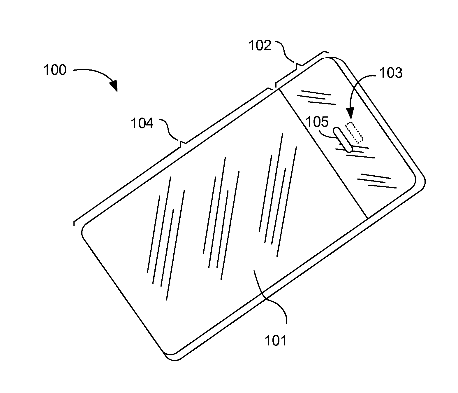
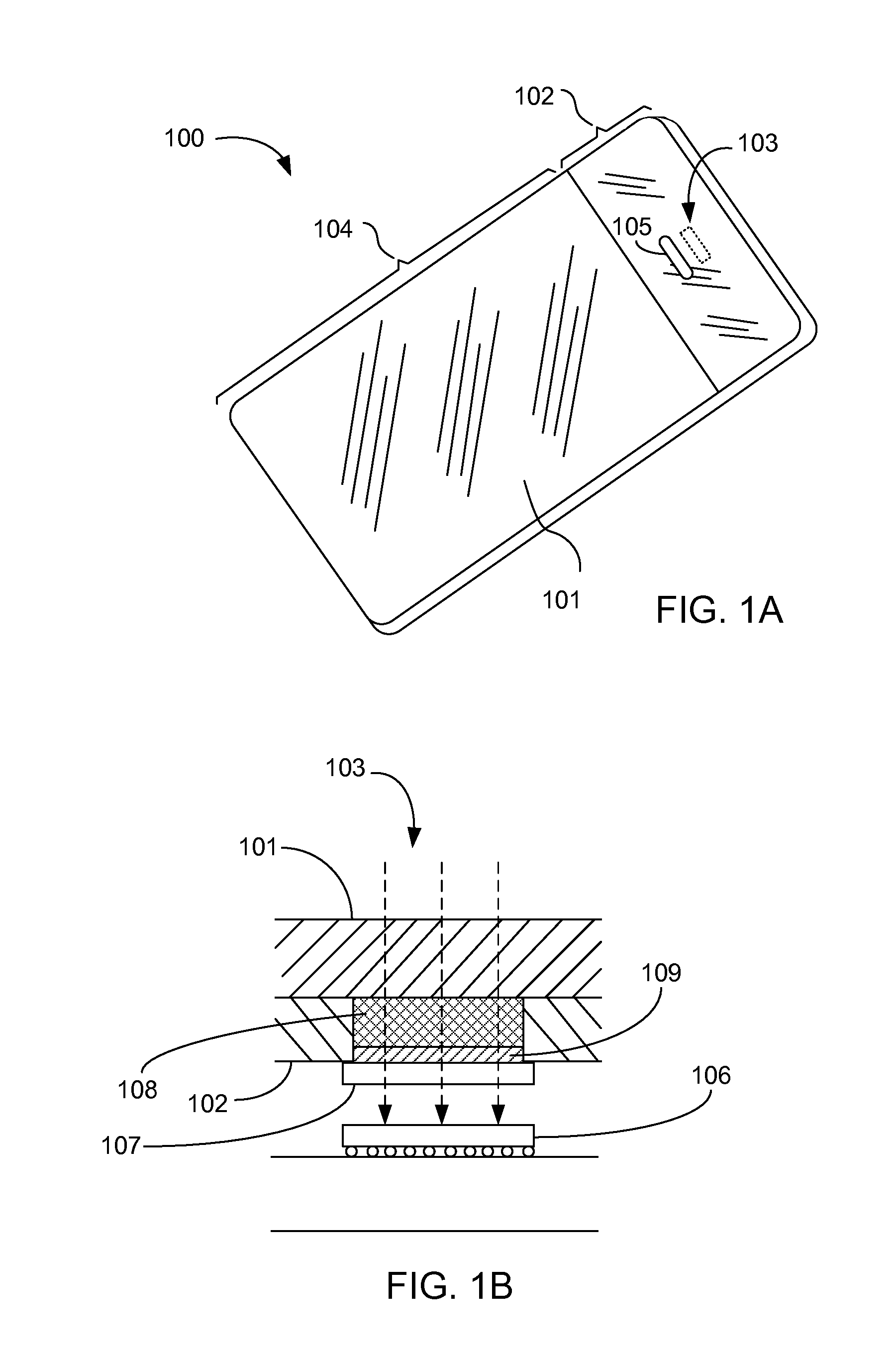
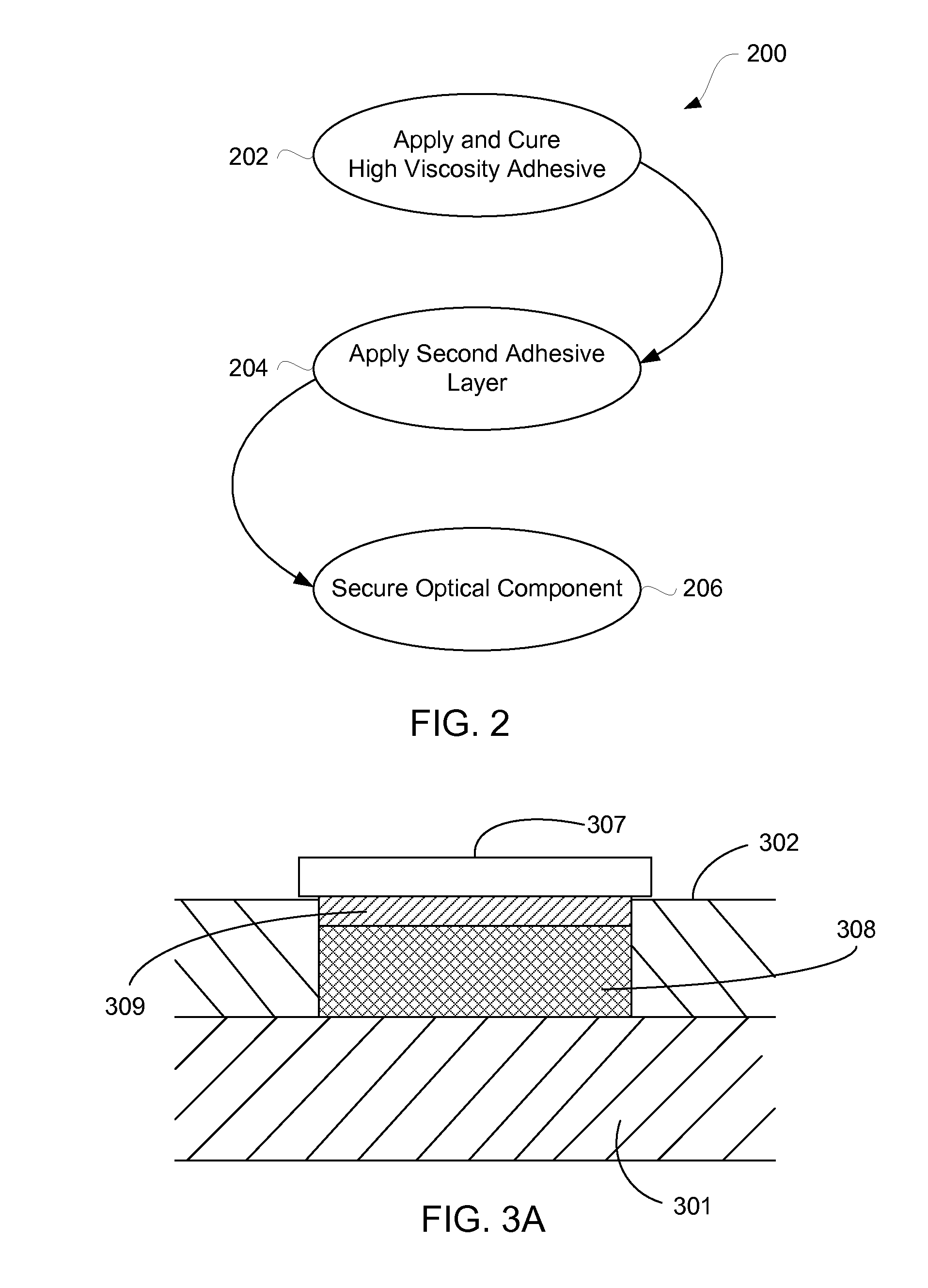
[0024]The invention pertains to assemblies using substrate materials, such as glass, and adhesives. The assemblies can be used in devices, such as electronic devices (e.g., portable electronic devices). The assemblies can be used to secure optical components to substrate materials. In one embodiment, a multi-layer adhesive stack can be used. The multi-layer adhesive stack can include a first layer of adhesive (e.g., self-leveling adhesive) that adhesively couples with a substrate material, which can be a cover glass for a portion of a housing for an electronic device. The multi-layer adhesive stack can also include a second layer of adhesive that is provided on the first layer of adhesive, after the first layer of adhesive has been cured. An optical component may be adhesively coupled with the second layer of adhesive such that the optical component is adhered to the substrate material by way of the multi-layer adhesive stack.

[0025]The following detailed description is illustrative ...


PUM

PropertyMeasurementUnit
viscosityaaaaaaaaaa
viscosityaaaaaaaaaa
viscosityaaaaaaaaaa

Abstract

Techniques or processes for producing assemblies using adhesives and substrate material, such as glass. In one embodiment, the assemblies may be for portable electronic devices. For example, a cover glass of a portable electronic device may have a first layer of a self-leveling adhesive, which may be adhesively coupled with the cover glass. A second layer of a second adhesive, which may be different than the self-leveling adhesive of the first layer, may be adhesively coupled with the first layer. An optical component may be adhesively coupled with the second layer, so as to secure the optical component. The first layer may be cured prior to securing the optical component, so that the optical component may be substantially isolated from stress effects of adhesive cure shrinkage of the first layer. Flexure, warpage or optical distortion of the optical component due to adhesive cure shrinkage may be substantially avoided.

Description

BACKGROUND OF THE INVENTION[0001]1. Field of the Invention[0002]This relates generally to assemblies using substrate materials, such as glass, and adhesives.[0003]2. Description of the Related Art[0004]Various assemblies and assembly methods are known. For example, precision machined optical housings and optical mounts have been used in optical assemblies and the like. Such arrangements may provide advantages in rugged assemblies with precise optical alignment. However, despite such advantages, further improvements may be needed. For example, such arrangements may be heavy or bulky. They also may be expensive, time consuming, or difficult to manufacture.[0005]Manufacturing challenges may be particularly difficult in the case of thin or low profile portable electronic devices that integrate one or more optical components. Examples of thin or low profile portable electronic devices that integrate optical components, and which have achieved great popularity with consumers, are the iPho...

Claims


Application Information

Patent Timeline
Patent Type & Authority Applications(United States)
IPC IPC(8): H05K7/00B32B17/06B05D5/10B32B7/02B31B1/62B31B50/62
CPCB05D5/10B32B7/02H05K7/00B32B7/12Y10T428/2809Y10T428/2848Y10T428/24959Y10T428/24851Y10T156/10B32B17/064B32B17/06
Inventor HUANG, WAYNE W.
Owner APPLE INC
Why Eureka
Try Eureka