Near-infrared absorbing film, optical filter comprising the same and electronic device

a near-infrared absorption and optical filter technology, applied in the direction of optical elements, instruments, coatings, etc., can solve the problems of insufficient near-infrared absorption capacity of sulfonate salt, insufficient use, and increase in viscosity, so as to reduce and/or prevent light in the near-infrared region effectively, prevent optical distortion effectively, thin thickness

Active Publication Date: 2021-07-27
SAMSUNG ELECTRONICS CO LTD
View PDF22 Cites 0 Cited by
  • Summary
  • Abstract
  • Description
  • Claims
  • Application Information

AI Technical Summary

Benefits of technology

[0008]Some example embodiments provide a near-infrared absorbing film having a thin thickness and capable of reducing or preventing optical distortion effectively.
[0045]The near-infrared absorbing film may have a thin thickness and may be capable of reducing and / or preventing light in a near-infrared region effectively; thus the near-infrared absorbing film may reduce and / or prevent optical distortion effectively.

Problems solved by technology

However, the copper sulfonate salt has very low near-infrared absorption capability (intensity), and thus has to be used in an excessive amount.
Therefore, viscosity increase during preparation of high concentration copper salt solution may be caused, which is not desirable for manufacture of a thin film.

Method used


Image

  • Near-infrared absorbing film, optical filter comprising the same and electronic device
  • Near-infrared absorbing film, optical filter comprising the same and electronic device
  • Near-infrared absorbing film, optical filter comprising the same and electronic device

Examples


example 1

[0155]Composition 1 is prepared by dispersing Dye 1 and an acrylic binder (HT1335, Samhwa Paints Industrial Co., Ltd.) in a solvent (methyl ethyl ketone).

[0156]Composition 2 is prepared by dispersing Copper Phosphate Salt 1 and an epoxy binder (EHPE 3150, DAICEL Corp.) in a solvent (methyl ethyl ketone).

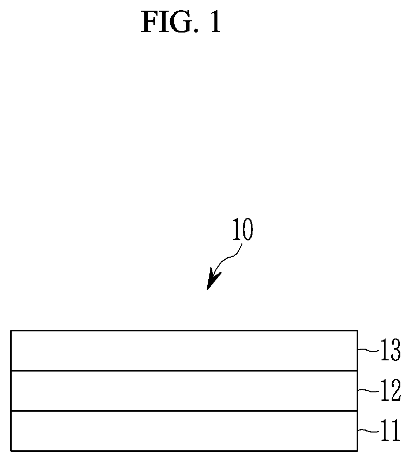
[0157]Composition 2 is bar-coated on a triacetyl cellulose film, dried at 85° C. for 1 minute, and thermally cured at 85° C. for 4 minutes to form a second near-infrared absorbing layer, and subsequently, Composition 1 is coated, dried, and thermally cured according to the same method as used for Composition 2 to form a first near-infrared absorbing layer on the second near-infrared absorbing layer and then, manufacture an optical filter (a triacetyl cellulose film / a second near-infrared absorbing layer / a first near-infrared absorbing layer).

example 2

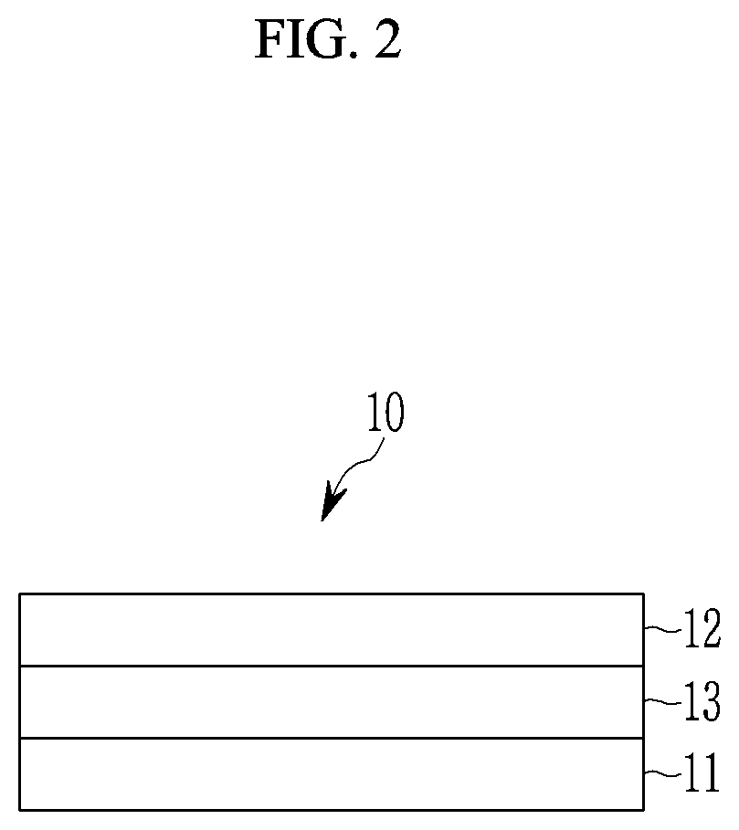
[0158]An optical filter is manufactured according to the same method as Example 1 except for changing a stacking order of the first near-infrared absorbing layer and the second near-infrared absorbing layer.

example 3

[0159]An optical filter is manufactured according to the same method as Example 1 except for using Dye 2 instead of Dye 1.


PUM

PropertyMeasurementUnit
wavelengthaaaaaaaaaa
light transmittanceaaaaaaaaaa

Abstract

Disclosed are a near-infrared absorbing film including a polymer film, a first near-infrared absorbing layer and a second near-infrared absorbing layer on the polymer film. The first near-infrared absorbing layer may be configured to transmit light in a visible region and to selectively absorb at least one part of light in a near-infrared region. The second near-infrared absorbing layer may be disposed on a surface of the first near-infrared absorbing layer. The first near-infrared absorbing layer may include a dye represented by Chemical Formula 1. The second near-infrared absorbing layer may include a copper complex compound. An optical filter may include the near-infrared absorbing film. An electronic device may include the optical filter.In Chemical Formula 1, R1 to R12 are described in the detailed description.

Description

CROSS-REFERENCE TO RELATED APPLICATION[0001]This application claims priority to Korean Patent Application No. 10-2018-0035224, filed in the Korean Intellectual Property Office on Mar. 27, 2018, the entire contents of which are incorporated herein by reference.BACKGROUND1. Field[0002]A near-infrared absorbing film, an optical filter including the same, and an electronic device including the optical filter are disclosed.2. Description of Related Art[0003]Recently, an electronic device including an image sensor that stores an image as an electrical signal, such as a cell phone, a digital camera, a camcorder and a camera, has been widely used.[0004]This electronic device may include an optical filter including a near-infrared absorbing film in order to reduce or prevent generation of an optical distortion by light in the other regions than a visible region.[0005]The near-infrared absorbing film is mounted in front of an image sensor of a camera module and thus plays a role of effectivel...

Claims


Application Information

Patent Timeline
Patent Type & Authority Patents(United States)
IPC IPC(8): G02B5/20G02B1/04G02B5/00H01L27/30G02B5/22C09B57/00
CPCG02B5/208G02B1/04G02B5/003G02B5/223H01L27/307C09B57/007C08J7/042C09D133/04C09D163/00C09D7/63C08J2301/10C08J2463/00C08J2433/04C08K5/3417C08K5/0091C09B67/009C08J5/18C08K5/0041C08K5/52H10K39/32
Inventor LEE, YONG JOOKIM, HYUNG JUNWON, JONG HOONKO, YOON SEOKJUNG, MYUNGSUP
Owner SAMSUNG ELECTRONICS CO LTD
Why Eureka
Try Eureka