Cmos-mems switch structure

a switch structure and micro-electromechanical technology, applied in the direction of contacts, relays, contact engagements, etc., can solve the problems of the switch structure b>100/b> still has many problems to be solved

Inactive Publication Date: 2012-11-08
NAT APPLIED RES LAB
View PDF5 Cites 7 Cited by
  • Summary
  • Abstract
  • Description
  • Claims
  • Application Information

AI Technical Summary

Benefits of technology

[0007]It is an object of the present invention to provide a CMOS-MEMS switch structure whose surface electrodes are made of an oxidation-resistant metal such as gold, tungsten, titanium, or nickel. Thus, the CMOS-MEMS switch structure is prevented from failure which may otherwise result from oxidation of the surface electrodes.

Problems solved by technology

However, as the major metal used in the CMOS manufacturing process is aluminum, which tends to oxidize and become an electrically insulating aluminum oxide when exposed to air, the surface electrodes of the resultant CMOS-MEMS switch elements may contact each other without effectively making electrical connection therebetween.
Therefore, the manufacture of the lateral contact-based CMOS-MEMS switch structure 100 still has many problems to be solved.

Method used


Image

  • Cmos-mems switch structure
  • Cmos-mems switch structure
  • Cmos-mems switch structure

Examples


Embodiment Construction

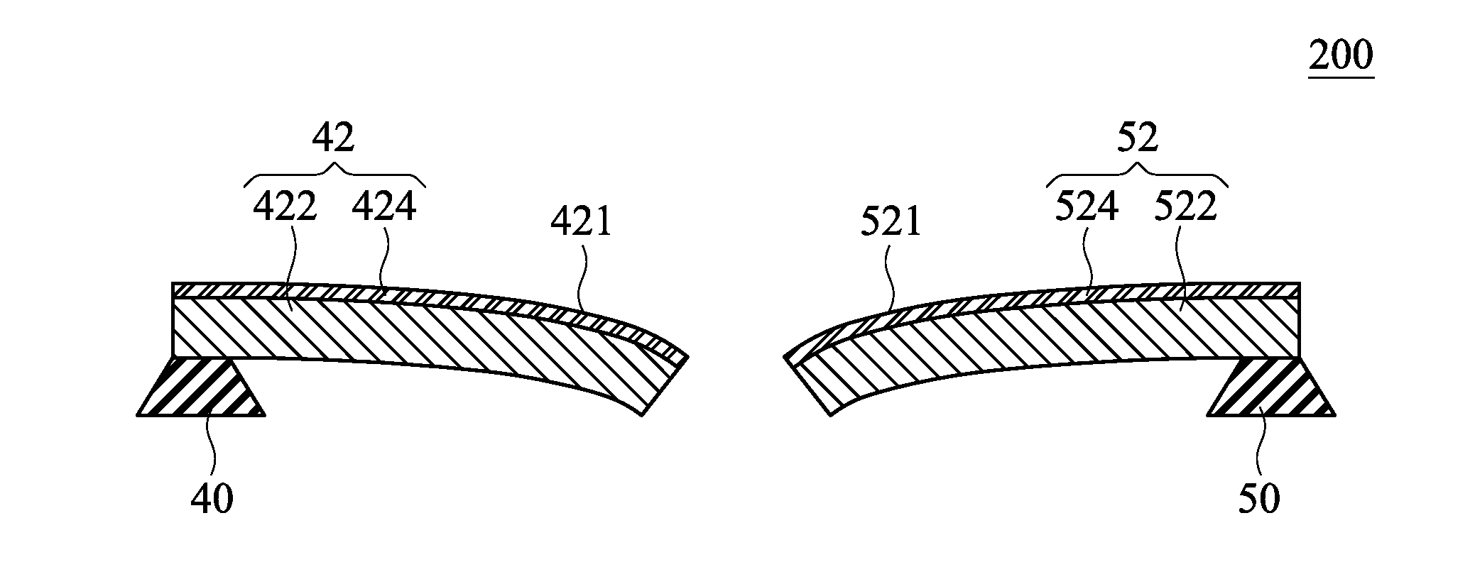
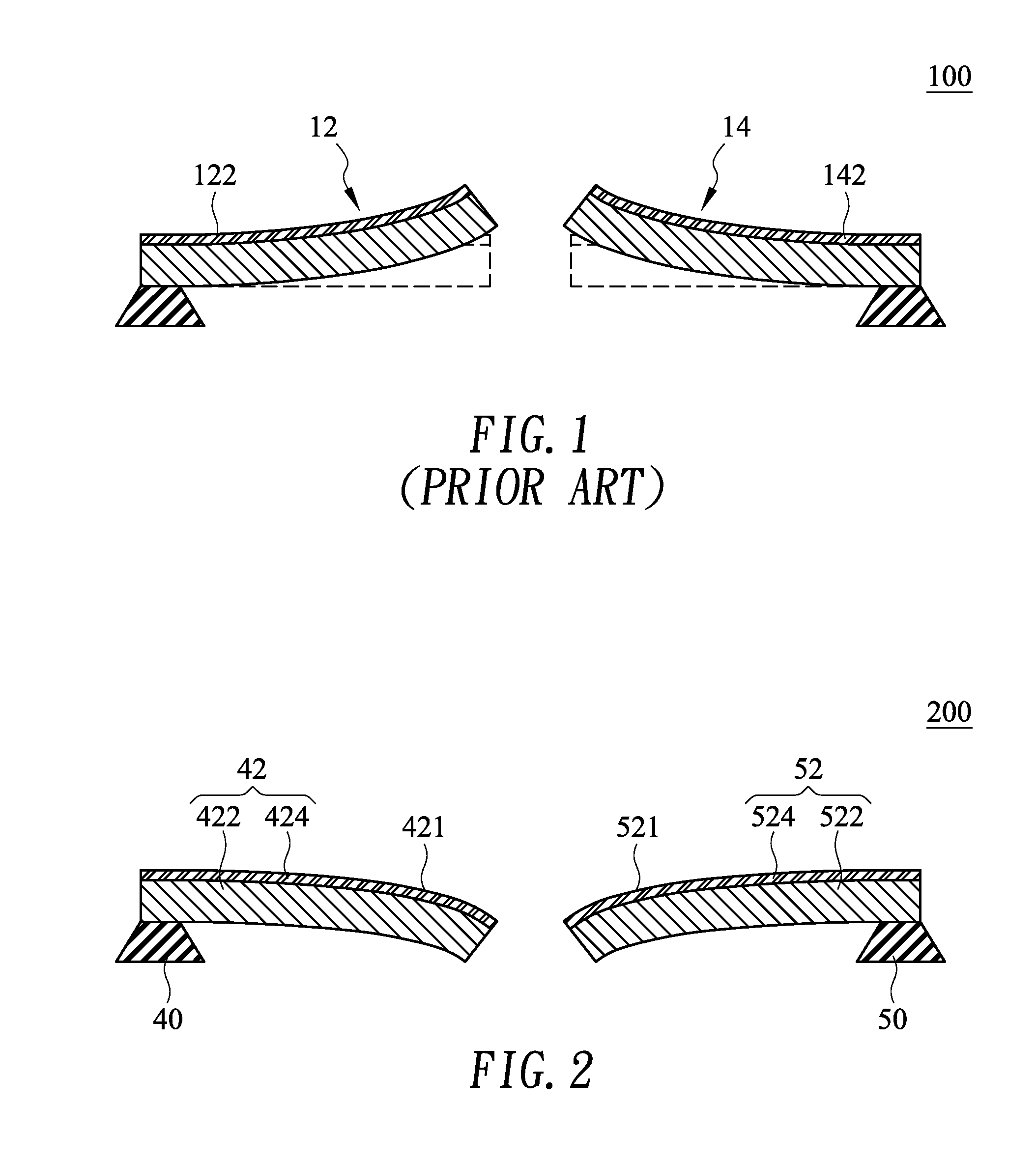
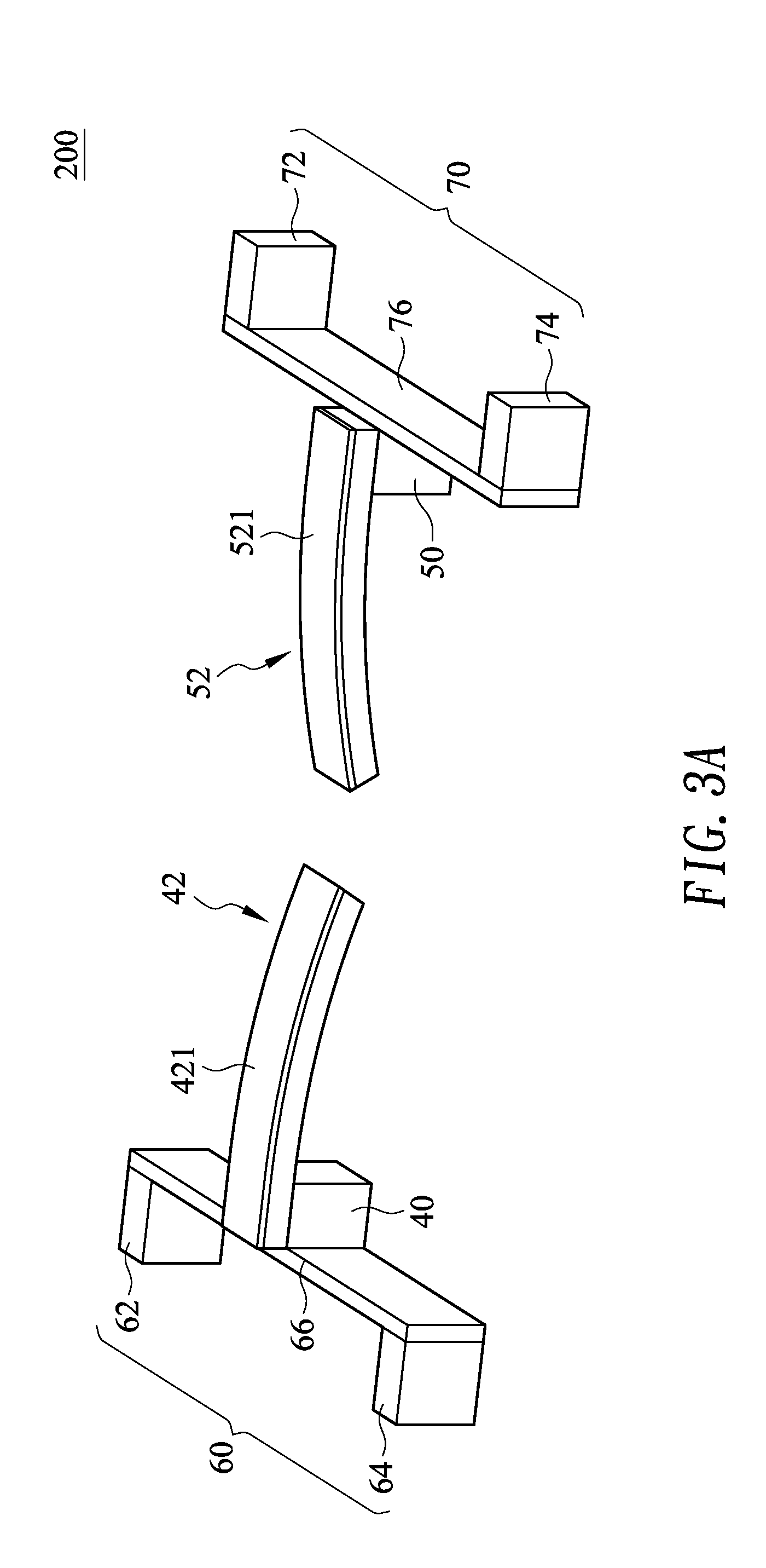
[0023]Referring to FIG. 2, a CMOS-MEMS switch structure 200 according to an embodiment of the present invention includes a first substrate 40, a second substrate 50, a first cantilever beam 42, and a second cantilever beam 52. The CMOS-MEMS switch structure 200 is made by a process incorporating both CMOS and MEMS manufacturing processes. For example, different layers of metals and oxides are stacked up using a standard 0.35-micron CMOS process. Then, MEMS element areas are defined on the stacked layers. Once the sacrificial layer arranged in the MEMS element areas is removed by etching, the desired MEMS structures are released. As the integrated CMOS-MEMS manufacturing processes have been developed to a very mature level, a detailed explanation of such processes is omitted, and only the resultant structure is described herein. It should be noted that all the materials of the disclosed CMOS-MEMS switch structure 200 are materials generally used in an integrated CMOS-MEMS manufacturi...


PUM


Abstract

A CMOS-MEMS switch structure is disclosed. The CMOS-MEMS switch structure includes a first substrate, a second substrate, a first cantilever beam, and a second cantilever beam. The first and second substrates are positioned opposite each other. The first cantilever beam is provided on the first substrate, extends from the first substrate toward the second substrate, and bends downward. Likewise, the second cantilever beam is provided on the second substrate, extends from the second substrate toward the first substrate, and bends downward. The first and second substrates are movable toward each other to connect a first top surface of the first cantilever beam and a second top surface of the second cantilever beam, and away from each other so that the first top surface of the first cantilever beam and the second top surface of the second cantilever beam are disconnected, thereby closing or opening the CMOS-MEMS switch structure.

Description

BACKGROUND OF THE INVENTION[0001]1. Technical Field[0002]The present invention relates to a microelectromechanical system (MEMS) switch structure and, more particularly, to a CMOS (complementary metal-oxide-semiconductor)-MEMS switch structure featuring integration of CMOS and MEMS technologies.[0003]2. Description of Related Art[0004]A switch for use in a telecommunication system must have high isolation and low insertion loss to prevent the system from noise interference and maintain system performance. Mechanical switches, for example, are preferred in telecommunication systems where high-frequency operation is required. Besides, as it is generally required that switches in a telecommunication system be more and more compact and lightweight, CMOS-MEMS switches which feature total compatibility with CMOS manufacturing processes have been developed.[0005]Typically, a CMOS-MEMS switch incorporating both CMOS and MEMS manufacturing processes is made by first performing a standard CMO...

Claims


Application Information

Patent Timeline
Patent Type & Authority Applications(United States)
IPC IPC(8): H01H59/00
CPCH01H1/0036H01H1/20H01L27/0617H01H2061/006H01H2001/0057H01H2001/0078H01H2001/0052
Inventor LAI, YOU-LIANGJUANG, YING-ZONGTSAI, HANN-HUEITSENG, SHENG-HSIANGCHIU, CHIN-FONG
Owner NAT APPLIED RES LAB
Why Eureka
Try Eureka