Polarization Direction of Optical Devices Using Selected Spatial Configurations

a spatial configuration and optical device technology, applied in the field of lighting techniques, can solve the problems of routine failure of conventional light bulbs, and inability to detect the direction of optical devices using selected spatial configurations, etc., to achieve the effect of easy detection for handling and often higher system efficiency

Active Publication Date: 2012-11-15
SLT TECH
View PDF3 Cites 32 Cited by
  • Summary
  • Abstract
  • Description
  • Claims
  • Application Information

AI Technical Summary

Benefits of technology

[0017]In another set of embodiments of the present invention, the method of determining the configuration of the strong and weak dipole planes of the die is used when combined with multiple die in an optical device in order to maximize light intensity.
[0019]Benefits are achieved by the present invention over conventional techniques. In one or more embodiments, the present device and method can provide a spatial orientation that is easily detectable for handling and packaging of die having strong and / or weak dipole planes. In other embodiments, the present device and method can be achieved using conventional technologies of scribing, breaking, and / or sawing / singulating. Preferably, the shaped die can be configured along with other die to form an array configuration. The array configuration is characterized by a system efficiency that is often higher than conventional unpolarized LEDs using c-plane GaN substrates in applications, which desire polarized emission. Depending upon the embodiment, one or more of these benefits may be achieved. These and other benefits are further described throughout the present specification and more specifically below.

Problems solved by technology

Unfortunately, drawbacks exist with the conventional Edison light bulb.
That is, the conventional light bulb dissipates much thermal energy.
Additionally, the conventional light bulb routinely fails often due to thermal expansion and contraction of the filament element.
Unfortunately, achieving high intensity, high-efficiency GaN-based green LEDs has been particularly problematic.
The performance of optoelectronic devices fabricated on conventional c-plane GaN suffer from strong internal polarization fields, which spatially separate the electron and hole wave functions and lead to poor radiative recombination efficiency.
Since this phenomenon becomes more pronounced in InGaN layers with increased indium content for increased wavelength emission, extending the performance of UV or blue GaN-based LEDs to the blue-green or green regime has been difficult.
Furthermore, since increased indium content films often require reduced growth temperature, the crystal quality of the InGaN films is degraded.
The difficulty of achieving a high intensity green LED has led scientists and engineers to the term “green gap” to describe the unavailability of such green LED.
In addition, the light emission efficiency of conventional GaN-based LEDs drops off significantly at higher current densities, as are required for general illumination applications, a phenomenon known as “roll-over.” Other limitations with blue LEDs using c-plane GaN exist.
These limitations include poor yields, low efficiencies, and reliability issues.

Method used


Image

  • Polarization Direction of Optical Devices Using Selected Spatial Configurations
  • Polarization Direction of Optical Devices Using Selected Spatial Configurations
  • Polarization Direction of Optical Devices Using Selected Spatial Configurations

Examples


Embodiment Construction

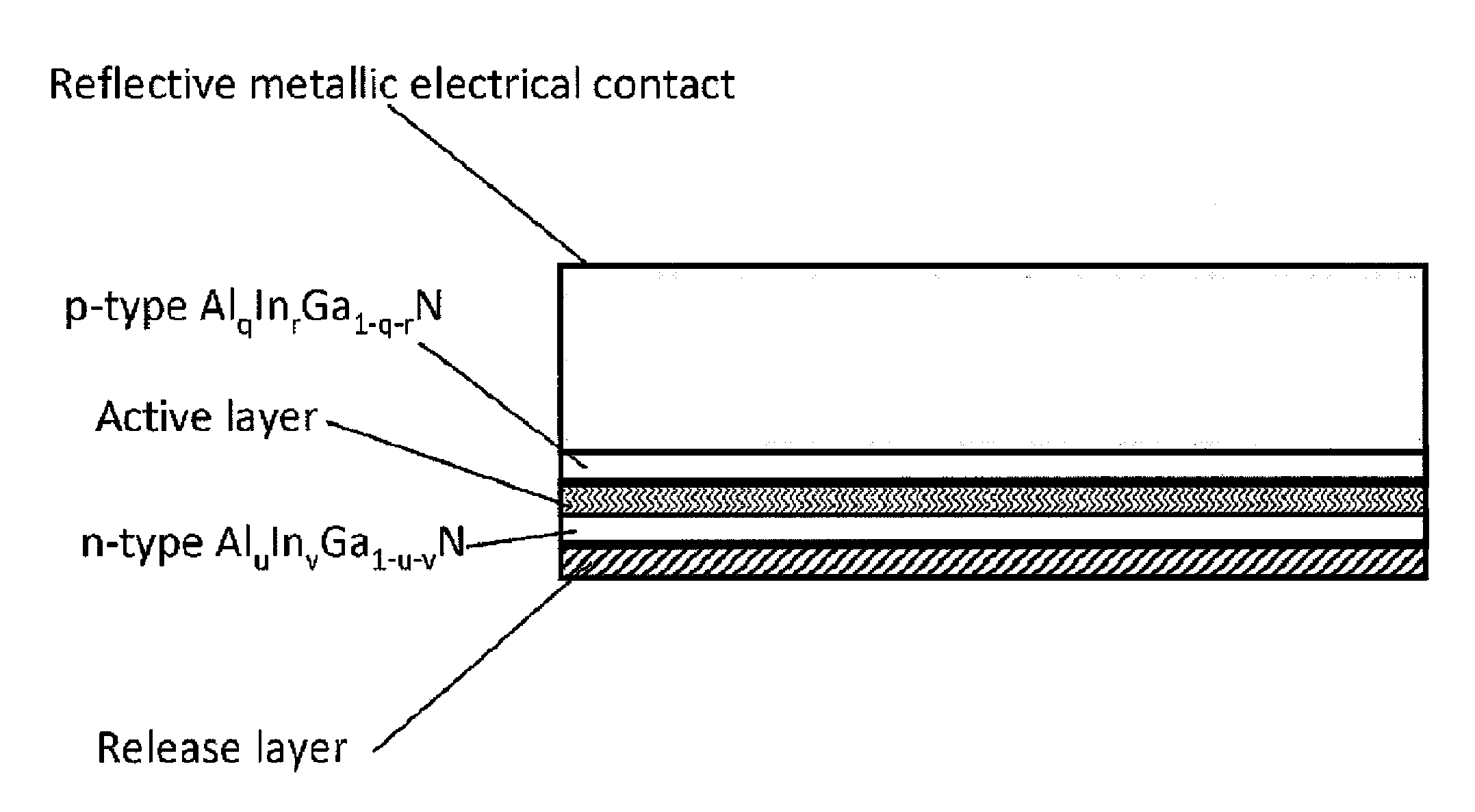
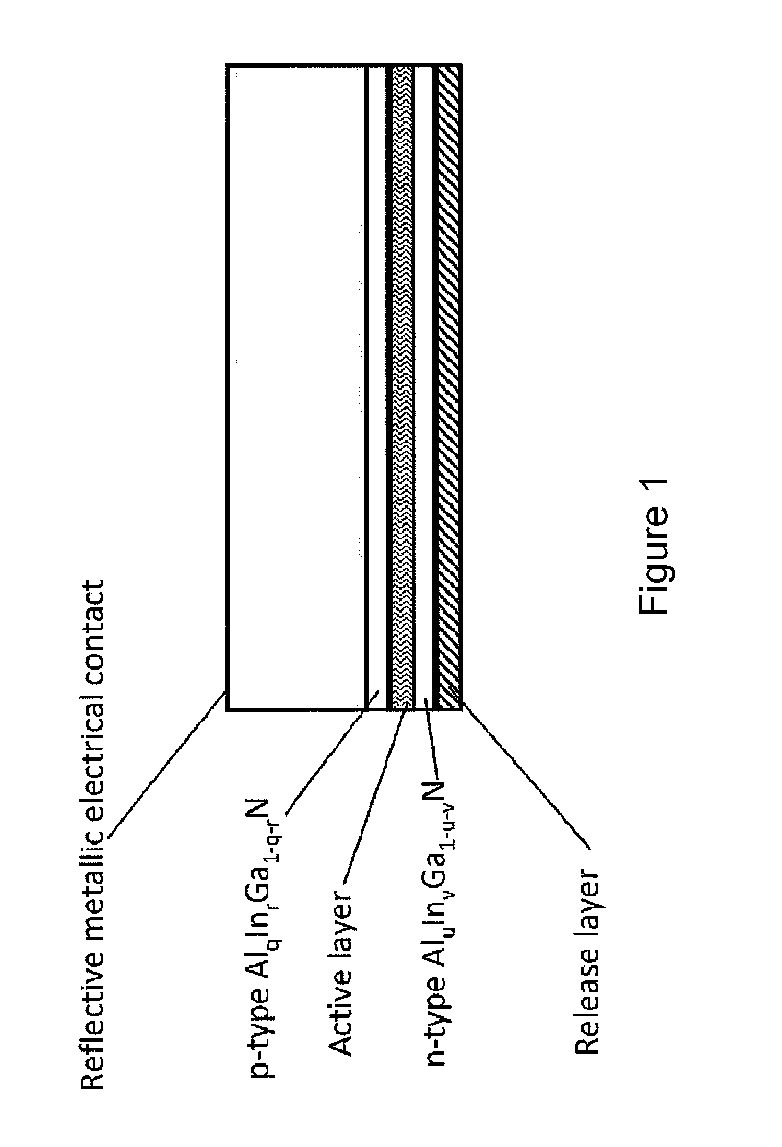
[0029]According to the present invention, methods and devices for the more efficient fabrication of optical devices are provided. More specifically, methods and devices for determining the configuration of the strong and weak emission dipole planes of the die made from GaN materials are provided. Merely by way of example, the invention can be applied to applications such as optoelectronic devices, and the like. Other applications that desire polarized emission include liquid crystal display (“LCD”) backlighting, liquid crystal on silicon (“LCOS”) lighting, selected applications of home and / or building lighting, medical applications, biological sampling, plant and algae growth, biofuels, microscopes, film and video (e.g., amusement, action, nature, in-door), multi-dimensional display or televisions, micro and / or pico displays, health and wellness, optical and / or data transmission / communication, security and safety, and others.

[0030]While conventional optical devices have been fabrica...


PUM


Abstract

A GaN based light emitting diode device which emits polarized light or light of various degrees of polarization for use in the creation of optical devices. The die are cut to different shapes, or contain some indicia that are used to represent the configuration of the weak dipole plane and the strong dipole plane. This allows for the more efficient manufacturing of such light emitting diode based optical devices.

Description

CROSS-REFERENCES TO RELATED APPLICATIONS[0001]This application claims priority to U.S. Provisional Application No. 61 / 158,622, filed Mar. 9, 2009, commonly assigned, and incorporated by reference for all purpose herein.BACKGROUND OF THE INVENTION[0002]The present invention relates generally to lighting techniques. More specifically, embodiments of the invention include techniques for the more efficient fabrication and handling of optical devices on semipolar or nonpolar crystalline semiconductor materials. Merely by way of example, the invention can be applied to applications such as white lighting, multi-colored lighting, general illumination, decorative lighting, automotive and aircraft lamps, street lights, lighting for plant growth, indicator lights, lighting for flat panel displays, other optoelectronic devices, and the like.[0003]In the late 1800's, Thomas Edison invented the light bulb. The conventional light bulb, commonly called the “Edison bulb,” has been used for over one...

Claims


Application Information

Patent Timeline
Patent Type & Authority Applications(United States)
IPC IPC(8): H01L33/30H01L33/08
CPCH01L33/16H01L33/32H01L33/20H01L33/18
Inventor SHARMA, RAJATHALL, ERIC M.
Owner SLT TECH
Why Eureka
Try Eureka